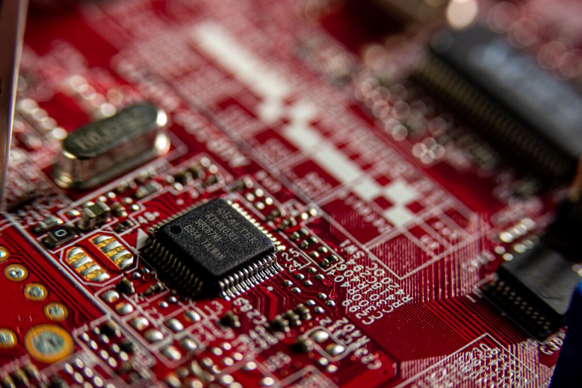
FinFET, or Fin Field-Effect Transistor, represents a significant advancement in semiconductor device architecture. Unlike traditional planar transistors, FinFETs employ a three-dimensional structure where the transistor’s channel is a raised silicon “fin.” The control gate wraps around three sides of this fin, providing superior electrostatic control over the channel. This design addresses fundamental limitations encountered as transistors continued to shrink.
The Planar Transistor Predecessor
Before FinFET, chipmakers relied on planar transistors, where the gate sat on top of a flat silicon channel. As these planar devices scaled down to smaller process nodes, they suffered from increasing short channel effects. These effects led to poor gate control over the channel, resulting in significant current leakage even when the transistor was intended to be off. This leakage wasted power and degraded performance.
The FinFET Innovation
The FinFET design mitigates these issues by elevating the channel into a fin-like structure. The gate then surrounds this fin on three sides, offering enhanced electrostatic control. This multi-gate approach effectively reduces unwanted current flow and improves switching speed, enabling continued transistor scaling. The industry adopted the FinFET process for many years, where the control gate is present on three sides of a raised channel.
How FinFET Architecture Works
FinFET technology fundamentally redefines how a transistor controls current flow. By moving from a two-dimensional to a three-dimensional structure, it provides a more effective means of modulating the channel. This architectural shift was essential for maintaining performance and power efficiency at advanced process nodes.
Channel Control and Leakage Reduction
The core of FinFET operation lies in its improved gate control. With the gate wrapping around three sides of the silicon fin, it exerts stronger electrostatic influence over the channel. This enhanced control significantly reduces leakage current, which is the unwanted current that flows through a transistor when it is supposed to be off. Reduced leakage directly translates to lower power consumption, a key advantage for modern electronic devices.
Scaling Benefits
FinFET architecture enabled the semiconductor industry to continue shrinking transistor dimensions, supporting process nodes from 22 nm down to 5 nm generations. This scaling allowed for higher transistor density on a chip, leading to more powerful and efficient integrated circuits. The ability to pack more transistors into the same area directly contributed to advancements in computing power.
Photo by Nic Wood on Pexels
Why Chipmakers Adopted FinFET
Chipmakers faced an impasse with planar transistor technology as the demand for smaller, faster, and more power-efficient chips grew. FinFET offered a viable path forward by addressing the inherent physical limitations of its predecessor. Its adoption was driven by the necessity to overcome these challenges and continue the trajectory of Moore’s Law.
Overcoming Planar Transistor Limitations
Planar transistors struggled with electrostatic constraints at smaller geometries, particularly below 28 nm. The gate’s inability to fully control the channel led to increased leakage and variability in transistor behavior. FinFET’s multi-gate structure provided the necessary electrostatic integrity to maintain control even at advanced nodes.
Power Efficiency and Performance
One of FinFET’s key advantages is improved control of leakage, the unwanted current that saps power. By minimizing this leakage, FinFET-based chips consume less power, extending battery life in mobile devices and reducing energy costs in data centers. This power efficiency, combined with faster switching speeds due to better channel control, delivered significant performance gains across various applications.
FinFET’s Role in Semiconductor Manufacturing
FinFET technology became the workhorse for advanced semiconductor manufacturing for over a decade. It facilitated the development of high-performance, low-power applications that define modern electronics. Its impact is evident in the capabilities of current computing devices.
Process Node Enablement
FinFET technology enabled the semiconductor industry to transition through several critical process nodes, specifically from 22 nm to 5 nm. This allowed chipmakers to continue delivering improvements in transistor density, speed, and power efficiency. Without FinFET, the scaling roadmap would have stalled much earlier.
Market Demand and Applications
The Fin Field Effect Transistor FinFET market encompasses advanced semiconductor devices designed for high-performance, low-power applications. As of early 2026, the semiconductor industry is experiencing a strong, AI-led upswing, with growth highly concentrated in Logic and Memory segments. FinFET-based chips power many of these devices, from high-end processors in servers to efficient mobile System-on-Chips (SoCs).
| Feature | Planar Transistor | FinFET Transistor |
|---|---|---|
| Gate Control | Limited (top surface only) | Excellent (three sides of channel) |
| Channel Structure | Flat, 2D | Raised fin, 3D |
| Leakage Current | Higher at small nodes | Significantly reduced |
| Scaling Capability | Limited below 28 nm | Enabled 22 nm to 5 nm nodes |
| Power Efficiency | Lower at small nodes | Higher |

Photo by ClickerHappy on Pexels
The Evolution Beyond FinFET
While FinFET proved revolutionary, its inherent design eventually faced new limitations as chipmakers pushed for even smaller geometries. The quest for continued scaling and performance improvements led to the development of successor technologies.
Electrostatic Constraints at Sub-5nm
FinFET technology, which enabled the 22 nm to 5 nm generations, begins to face electrostatic constraints in the sub-5 nm regime. At these extremely small dimensions, even the three-sided gate control becomes insufficient to fully mitigate short channel effects and leakage. The physical limits of the fin structure itself become a bottleneck.
Transition to Gate-All-Around (GAA)
The industry is now transitioning from FinFET to Gate-All-Around (GAA) transistor architectures, particularly at the 2 nm node. GAA transistors completely surround the channel with the gate, offering even greater electrostatic control than FinFETs. This transition introduces a step-function increase in three-dimensional structural complexity, requiring advanced manufacturing tools.
Key Takeaways
- FinFET technology introduced a 3D transistor structure with a gate wrapping around three sides of a silicon fin.
- This design significantly improved electrostatic control over the transistor channel, reducing leakage current.
- FinFET enabled continued scaling of semiconductor devices, supporting process nodes from 22 nm down to 5 nm.
- Its adoption was driven by the need to overcome power leakage and performance degradation in planar transistors.
- While successful, FinFET faces electrostatic limits below 5 nm, leading to the adoption of Gate-All-Around (GAA) transistors.
The shift to FinFET was not merely an incremental improvement but a fundamental architectural change, allowing the semiconductor industry to extend Moore’s Law for over a decade when planar scaling had reached its physical limits.
Semiconductor Growth Concentration (2026)
Logic: 60% of total growth | Memory: 30% of total growth | Other: 10% of total growth — Source: Semiconductors in 2026: The AI‑Driven Upswing Meets …
Real World Example
Modern high-performance processors found in personal computers, smartphones, and data center servers extensively utilize FinFET technology. For instance, many CPUs and GPUs manufactured at 16 nm, 10 nm, and 7 nm process nodes rely on FinFETs to achieve their balance of speed and power efficiency. These chips power demanding applications like artificial intelligence workloads, advanced gaming, and complex simulations. The low leakage characteristics of FinFETs are particularly beneficial for mobile devices, extending battery life while maintaining high computational power.
Frequently Asked Questions
What is the primary advantage of FinFET over planar transistors?
The primary advantage of FinFET is its superior electrostatic control over the transistor channel. By wrapping the gate around three sides of a raised silicon fin, it significantly reduces leakage current and improves switching performance compared to planar designs.
Which process nodes did FinFET technology enable?
FinFET technology was instrumental in enabling the semiconductor industry to scale down to advanced process nodes. It supported manufacturing generations ranging from 22 nanometers down to 5 nanometers, allowing for denser and more efficient chips.
Why is FinFET being replaced by Gate-All-Around (GAA) transistors?
FinFET technology begins to face electrostatic constraints at sub-5 nanometer dimensions, where its three-sided gate control becomes insufficient. Gate-All-Around (GAA) transistors offer even greater control by completely surrounding the channel, addressing these limitations for future scaling.
How does FinFET contribute to power efficiency?
FinFET contributes to power efficiency by drastically reducing leakage current, which is the unwanted flow of electricity when a transistor is supposed to be off. This reduction means less wasted power, leading to lower energy consumption for devices and longer battery life.

SiliconeUpdate.com is a technology news platform that publishes updates and informational content related to silicon technology, software, artificial intelligence, and emerging technologies.
All articles published on this platform are attributed to SiliconeUpdate.com instead of individual authors. Content is presented in a neutral, informational format without personal opinions.
—
Content Publishing
SiliconeUpdate.com publishes news and updates based on publicly available information, official announcements, and industry developments. The focus is on clarity, relevance, and timely reporting.
—
Editorial Control
All editorial decisions, updates, and content management are handled at the platform level. No individual human or AI identity is presented as the author of articles.
—
Contact
For editorial communication or general queries, contact:
Email: neemasharma@gmail.com