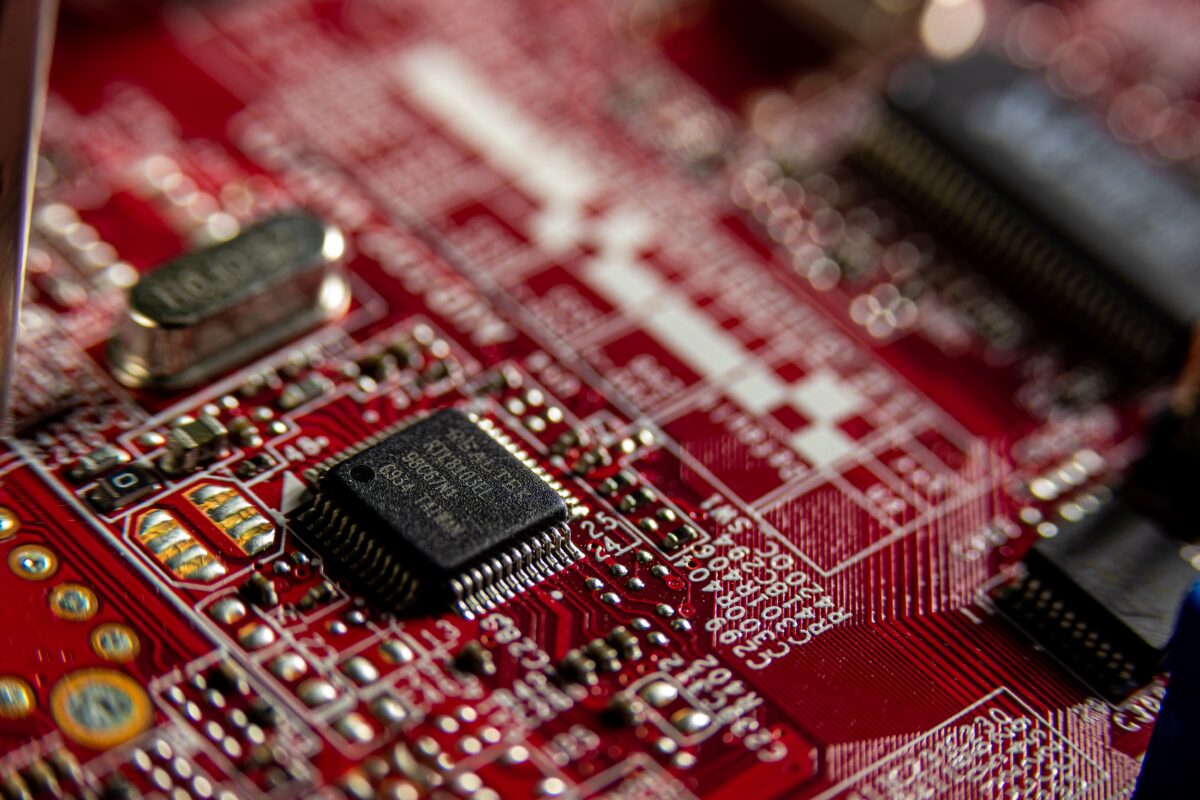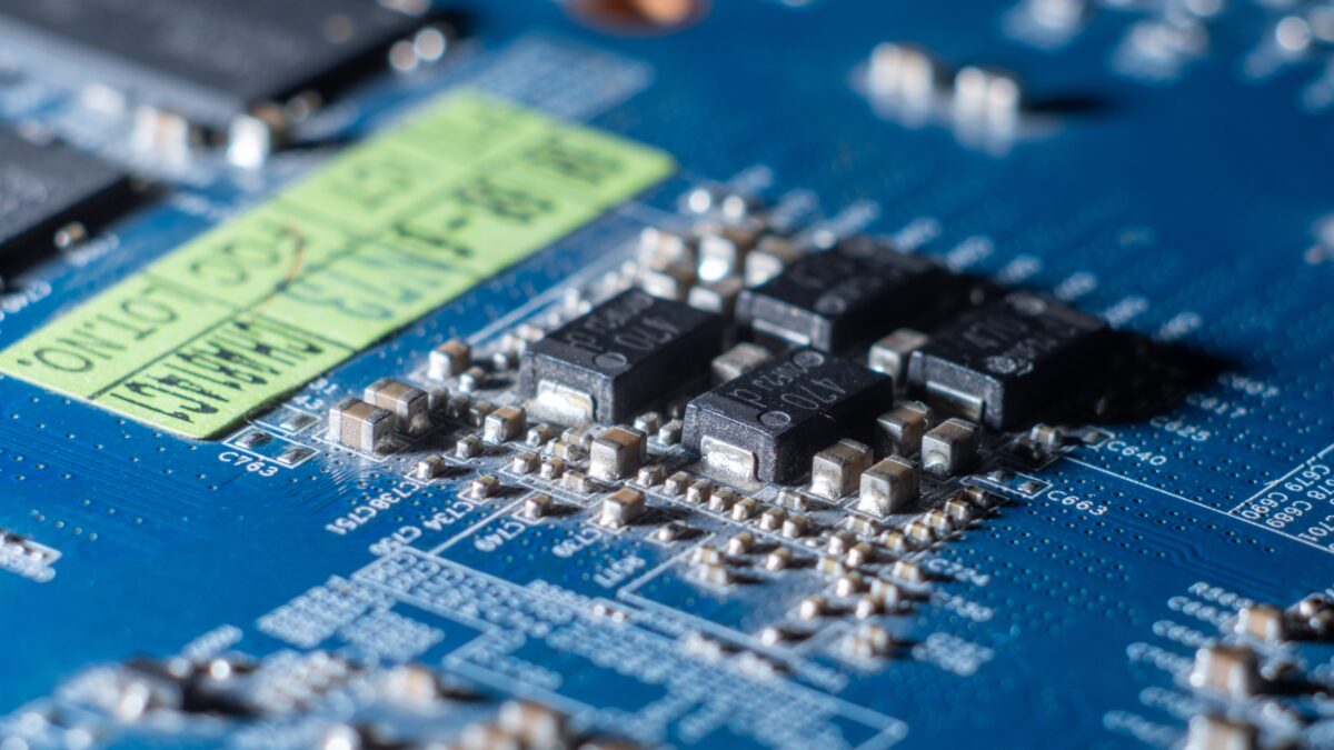
Semiconductor manufacturing transforms raw silicon into complex integrated circuits, commonly known as chips. This intricate process involves hundreds of steps, categorized into two primary phases: front-end manufacturing and back-end manufacturing. The journey begins with a bare silicon wafer and culminates in a fully functional, tested chip ready for integration into electronic devices.
From Silicon to Substrate
The foundation of every semiconductor chip is a highly purified silicon crystal. This crystal is grown into large ingots, which are then sliced into thin, circular discs called wafers. These wafers serve as the substrate upon which microscopic electronic circuits will be built.
The Manufacturing Overview
The manufacturing process is broadly divided into two main stages. The front-end process focuses on forming fine circuit patterns and transistors directly onto the silicon wafer. Following this, the back-end process involves separating these individual circuits, packaging them, and conducting final tests to ensure functionality and reliability.
The Front-End Process: Wafer Fabrication
The front-end process, also known as wafer fabrication, is a series of manufacturing steps that create the transistors and interconnections on a silicon wafer. This stage is where the fundamental computing elements are formed, defining the chip’s functionality.
Photolithography: Pattern Transfer
Photolithography is central to pattern transfer, using light to project circuit designs onto the wafer. A photosensitive material, called photoresist, is applied to the wafer, exposed to light through a mask, and then developed to create the desired pattern. Cutting-edge lithography systems, such as those utilizing extreme ultraviolet (EUV) light, are supported by advanced vacuum solutions, as recognized by the John Munck Award 2026 for delivering higher precision.
Etching and Deposition: Building Layers
After patterning, etching removes unwanted material from the wafer, defining the circuit features. Conversely, deposition processes add new layers of material, such as insulators or conductors, onto the wafer. These alternating steps of patterning, etching, and deposition build the complex, multi-layered structures of transistors and interconnects.
Doping: Modifying Electrical Properties
Doping introduces impurities into specific regions of the silicon wafer to alter its electrical conductivity. This process creates N-type and P-type semiconductor regions, which are essential for forming the junctions and channels within transistors. Precise control over doping concentrations is critical for device performance.

Photo by Zafer Erdoğan on Pexels
Key Technologies in Front-End Manufacturing
Achieving the intricate patterns and structures required for modern chips relies on highly advanced and specialized technologies.
Advanced Lithography Systems
The continuous demand for smaller, more powerful chips drives innovation in lithography. Extreme Ultraviolet (EUV) lithography is a key technology enabling the creation of increasingly finer circuit patterns. Solutions supporting these systems, like the groundbreaking extreme ultraviolet vacuum solution celebrated by the John Munck Award 2026, are vital for delivering higher throughput and precision.
Cleanroom Environments
Semiconductor fabrication occurs in highly controlled cleanroom environments to prevent contamination. Even microscopic dust particles can cause defects on the tiny circuit patterns, rendering a chip non-functional. These facilities maintain stringent air purity standards, often thousands of times cleaner than a typical operating room.
The Back-End Process: Assembly and Testing
Once the front-end process completes the circuit patterns on the wafer, the back-end manufacturing phase begins. This stage transforms the patterned wafer into individual, functional chips ready for use.
Wafer Dicing and Die Separation
After all front-end processing is complete, the wafer contains hundreds or thousands of identical circuits, called dies. A precision saw cuts the wafer into these individual dies, a process known as wafer dicing. Each die represents a single, unpackaged chip.
Packaging: Protecting the Die
Individual dies are fragile and require protection and external connectivity. Packaging involves enclosing the die in a protective casing, typically made of plastic or ceramic. This package also provides the electrical connections (pins or balls) that allow the chip to interface with a circuit board.
Final Testing and Quality Assurance
Before shipment, every packaged chip undergoes rigorous final testing. These tests verify electrical functionality, performance, and reliability under various conditions. Chips are often sorted, or “binned,” based on their performance characteristics, ensuring they meet specific product specifications.

Photo by Tima Miroshnichenko on Pexels
The Role of Foundries in Chip Production
The semiconductor industry often separates chip design from manufacturing, with specialized facilities handling production.
Contract Manufacturing Model
A foundry is a factory that manufactures semiconductor chips on wafers, typically on a contract basis for other companies. This model allows companies to focus on chip design without the immense capital investment required for fabrication facilities. The U.S. Semiconductor Ecosystem Map defines a foundry as a facility available on a contract basis.
Industry Impact and Investment
The foundry model contributes to a dynamic semiconductor ecosystem, supporting diverse innovation. The 2026 global semiconductor industry outlook projects soaring sales, with a shifting focus toward risk mitigation, integrated systems, and balanced investment across the supply chain, including foundry services. This strategic investment ensures robust production capabilities for future demand.
| Process Phase | Primary Goal | Key Steps | Environment |
|---|---|---|---|
| Front-End Manufacturing | Forming microscopic circuit patterns and transistors on a silicon wafer. | Photolithography, Etching, Deposition, Doping, Planarization. | Ultra-cleanroom (Class 1-10), highly controlled temperature/humidity. |
| Back-End Manufacturing | Separating, packaging, and testing individual dies into functional chips. | Wafer Dicing, Die Bonding, Wire Bonding, Encapsulation, Final Test. | Cleanroom (Class 100-1000), less stringent than front-end. |
Key Takeaways
- Semiconductor manufacturing is a multi-stage process transforming silicon wafers into functional chips.
- The front-end process involves wafer fabrication, creating transistors and circuits through photolithography, etching, deposition, and doping.
- Advanced technologies like EUV lithography and stringent cleanroom environments are critical for front-end precision.
- The back-end process focuses on dicing wafers into individual dies, packaging them for protection and connectivity, and conducting final electrical tests.
- Foundries operate on a contract basis, manufacturing chips for design companies and playing a vital role in the global semiconductor supply chain.
The sheer scale of precision in semiconductor manufacturing is astounding; a single dust particle, invisible to the naked eye, can render an entire complex chip useless during the front-end fabrication process.
Real World Example
Consider the production of a modern smartphone processor. The journey begins with a large silicon ingot, grown and sliced into thin wafers. In a specialized foundry, these wafers undergo hundreds of front-end steps, where layers of silicon, insulators, and metals are precisely patterned using EUV lithography, etched, and deposited to form billions of transistors and interconnects. This intricate process takes several weeks, with each wafer passing through numerous machines in a meticulously controlled cleanroom environment.
Once the front-end is complete, the wafer is moved to the back-end facility. Here, it is carefully cut into individual processor dies. Each die is then mounted onto a substrate, tiny wires are bonded to connect it to the package, and it is encapsulated in a protective casing. Finally, the packaged processor undergoes extensive electrical and functional testing to ensure it meets performance specifications before being shipped to a smartphone manufacturer for integration.
Frequently Asked Questions
What is a silicon wafer?
A silicon wafer is a thin, circular slice of highly purified silicon crystal, serving as the substrate for building integrated circuits. It is the starting material for semiconductor manufacturing, upon which all chip components are fabricated.
What is the difference between front-end and back-end manufacturing?
Front-end manufacturing involves creating the actual electronic circuits and transistors on the silicon wafer. Back-end manufacturing focuses on separating these circuits into individual dies, packaging them, and performing final tests to prepare them for use.
Why are cleanrooms essential in chip manufacturing?
Cleanrooms are essential because even microscopic dust particles can cause defects on the tiny circuit patterns being created on the wafer. These controlled environments maintain extremely low levels of airborne particulates to ensure high manufacturing yields and chip reliability.
What role do foundries play in the semiconductor industry?
Foundries are specialized factories that manufacture semiconductor chips on a contract basis for other companies. They provide the immense capital investment and technical expertise required for fabrication, allowing chip design firms to focus solely on innovation and intellectual property.
SiliconeUpdate.com is a technology news platform that publishes updates and informational content related to silicon technology, software, artificial intelligence, and emerging technologies.
All articles published on this platform are attributed to SiliconeUpdate.com instead of individual authors. Content is presented in a neutral, informational format without personal opinions.
—
Content Publishing
SiliconeUpdate.com publishes news and updates based on publicly available information, official announcements, and industry developments. The focus is on clarity, relevance, and timely reporting.
—
Editorial Control
All editorial decisions, updates, and content management are handled at the platform level. No individual human or AI identity is presented as the author of articles.
—
Contact
For editorial communication or general queries, contact:
Email: neemasharma@gmail.com