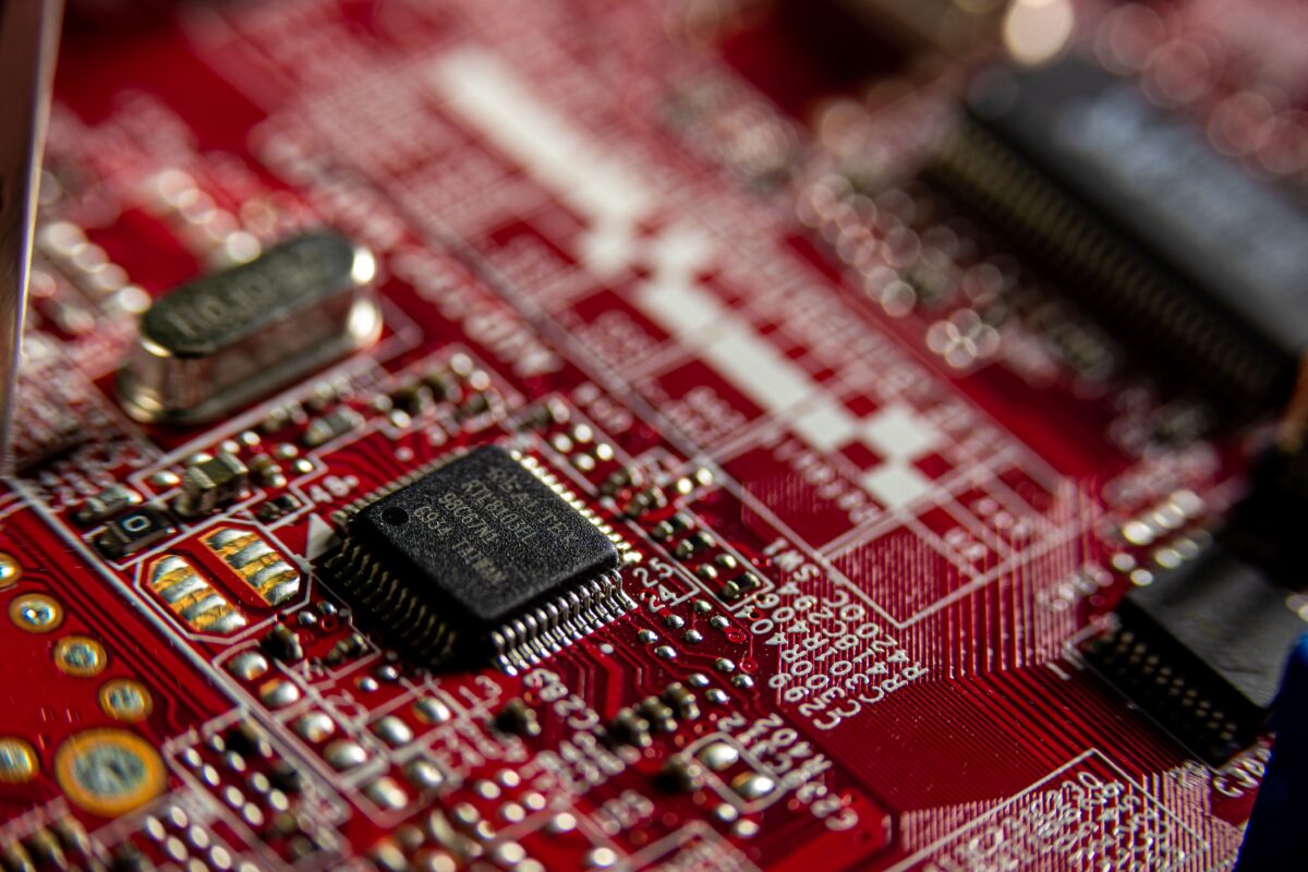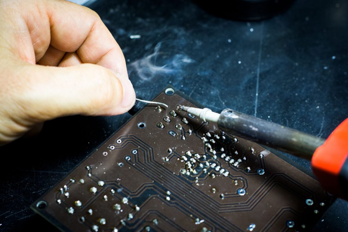
Every new chip generation is harder than the last, but 2nm-class manufacturing is a particularly steep climb. The industry is changing its transistor design, pushing lithography tools to their limits, and squeezing patterns so small that single stray particles and random photon effects can ruin a chip. The result is chips that cost more, take longer to ramp, and can be made by only a few companies. For more on the industry behind them, see our semiconductor and AI chip coverage.
A new transistor design
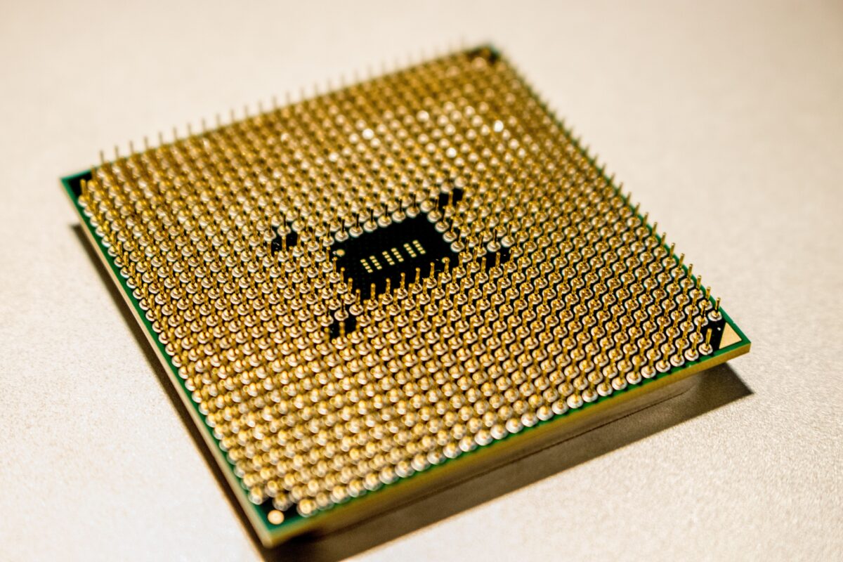
The first difficulty is that 2nm is not just a smaller version of the previous node. The industry is moving from FinFET to gate-all-around nanosheet transistors, which we introduced in the race to build smaller semiconductor nodes. Instead of one vertical fin, a GAA device stacks several horizontal nanosheets, and the gate material must wrap around every one of them.
That creates new manufacturing problems. A 2026 technical review points out that the process requires a full gate-all-around fill, in which high-k dielectric and work-function metals must coat every surface of the stacked sheets, including the narrow gaps between them. Another overview adds that variability in nanosheet thickness can affect performance, so uniformity across the whole wafer becomes critical.
A small error in how thick a layer is, or how evenly it is filled, can change a transistor’s behavior. At billions of transistors per chip, those small variations decide whether a chip works.
Lithography at the limit
The second difficulty is printing the patterns. Leading-edge chips depend on extreme ultraviolet (EUV) lithography, which SemiEngineering’s reporting describes as one of the biggest barriers to scaling production. Even microscopic defects can distort reflected light and cause patterning failures, which drives up defect rates and cuts yield.
EUV also brings a problem that older tools didn’t have: randomness. Lithography expert Chris Mack explains that with EUV, yield suffers because of stochastic effects such as line-edge roughness and contact-hole roughness, caused by photon shot noise and other sources. At these dimensions, there are so few photons per feature that statistical variation can create missing holes or tiny bridges between lines. A 2026 engineering overview lists stochastic defects and overlay errors among the main hurdles, since overlay errors stack across layers and can kill yield long before anything looks wrong under a microscope.
The machines add to the pressure. One report puts the price of an ASML low-NA EUV scanner at about $235 million and a high-NA system at about $380 million. High-NA tools offer better resolution, but another analysis notes that their cost forces foundries to keep stretching standard low-NA EUV with complicated multi-patterning, and that TSMC has delayed wide adoption of high-NA for economic reasons. We covered that decision in the race to build smaller semiconductor nodes.
Defects you can’t see
Cleanliness matters more as features shrink. One industry newsletter describes how, at 2nm, a particle too small to see can destroy thousands of transistors, since every major step, from lithography to etch to deposition, exposes the wafer. EUV masks are vulnerable too. A patent on mask defects notes that because one mask is used over and over, any multilayer defect affects every device made with it.
Backside power adds another layer
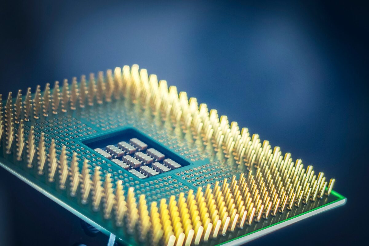
Some 2nm-class processes also move power delivery to the back of the wafer, which solves some problems and creates others. A description of TSMC’s A16 notes that it introduces backside wafer thinning, precise alignment for the power-rail contacts, and defect control in nanosheet stacking. The same overview says TSMC deferred this feature past the first N2 version to prioritize quick validation of the nanosheet design and manage complexity during the ramp.
Intel took the opposite approach by combining GAA and backside power in 18A. An analysis of the three strategies argues this means accepting all of these costs at once, which it says explains why 18A carries the highest yield and schedule risk. That is one analyst’s view, but it shows why two big changes at once is risky.
Yields and learning curves
Getting a new node to produce good chips in volume takes time. One 2026 overview says initial yields may be low, though TSMC reports improvements, and that Samsung’s SF2 yields were reported around the 50 percent range versus 60 to 80 percent for TSMC’s N2 in early reports. Treat such numbers cautiously: foundries guard yield data closely, and these figures come from a secondary source rather than company disclosures.
Yield drives cost directly. SemiEngineering quotes an industry expert saying that most of the cost of a mask blank is driven by yield, and the same logic applies to wafers: when fewer chips on a wafer work, each good chip costs more.
Cost and capacity
All of this raises prices. One report says 5nm and 3nm wafers have exceeded $20,000 and that a 2nm wafer is predicted to reach about $30,000, though such forecasts vary. Because AI customers value performance per watt, an analysis from Exponential Industry argues foundries can pass higher wafer costs on to hyperscalers.
The equipment bottleneck limits how fast capacity can grow. The same newsletter that describes invisible particles estimates that a large 2nm fab could need more than 300 EUV machines, while ASML is the sole supplier and makes only about 50 a year. That is an illustrative estimate from a newsletter, not an ASML figure, but it shows why building a new leading-edge fab takes so long. It also helps explain why only a few companies can compete, and why 2nm lead times are so long. We examined those constraints in why semiconductor supply chains matter for AI.
Smaller doesn’t mean easier gains
The payoff for all this effort is shrinking, too. EE Times quotes an analyst saying TSMC’s N2 delivers strong speed and power gains but only a mediocre density improvement over N3E. In other words, the industry is paying more for each step while getting less from raw shrinking, which is why packaging and memory have become equally important.
Still, the demand is there. TSMC’s own Q2 2026 results show 2nm already accounting for 3 percent of wafer revenue, and AI customers keep pushing for more efficiency, a need we described in why AI data centers need much more power. As we covered in why TSMC is so important to the global AI industry, the company that can master these problems at scale holds an enormous advantage.
The bigger picture
2nm chips are harder to make because every part of the process is pushed at once: a new transistor structure, tools operating near their physical limits, random effects that can’t be fully controlled, new power delivery techniques, and defects too small to see. The cost shows up in wafer prices, long lead times, and a shrinking list of companies that can compete. For the AI industry, that means the best chips will remain scarce and expensive, and the firms that solve manufacturing first will shape what AI hardware can do. Follow our AI hardware coverage as 2nm ramps and the industry looks toward what comes next.

SiliconeUpdate.com is a technology news platform that publishes updates and informational content related to silicon technology, software, artificial intelligence, and emerging technologies.
All articles published on this platform are attributed to SiliconeUpdate.com instead of individual authors. Content is presented in a neutral, informational format without personal opinions.
—
Content Publishing
SiliconeUpdate.com publishes news and updates based on publicly available information, official announcements, and industry developments. The focus is on clarity, relevance, and timely reporting.
—
Editorial Control
All editorial decisions, updates, and content management are handled at the platform level. No individual human or AI identity is presented as the author of articles.
—
Contact
For editorial communication or general queries, contact:
Email: neemasharma@gmail.com