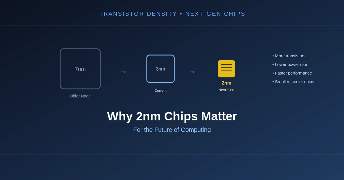
For years, semiconductor companies have been pushing transistor sizes from one process generation to the next: 14nm, 10nm, 7nm, 5nm, and 3nm. The industry is now moving into the 2nm era.
But what does 2nm actually mean, and why does it matter?
A 2nm chip is not simply a smaller version of a 3nm chip. Modern process nodes are no longer a straightforward measurement of one physical transistor dimension. Instead, the name generally identifies a new generation of semiconductor manufacturing technology that aims to improve a combination of performance, power efficiency, transistor density, and design capabilities.
That matters because modern computing is running into a difficult problem: we want more AI performance, faster smartphones, more capable servers, and increasingly powerful data centers, but we cannot keep increasing power consumption at the same rate.
2nm technology is one of the ways the semiconductor industry is trying to continue increasing computing capability while controlling energy use.
What Is a 2nm Chip?
A 2nm chip is a semiconductor manufactured using a process technology commonly referred to as a 2nm process node.
The important point is that “2nm” should not be interpreted as every transistor being exactly 2 nanometers wide.
Modern process-node names are technology-generation labels rather than a single physical measurement. A 2nm process involves improvements across transistor architecture, density, interconnects, power delivery, manufacturing processes, and design rules.
For example, TSMC’s N2 technology uses a nanosheet transistor architecture, moving beyond the FinFET architecture used by its earlier generations. TSMC says its N2 technology entered volume production in the fourth quarter of 2025.
This transition is important because shrinking conventional transistor structures becomes increasingly difficult as dimensions become extremely small.
Why Do Transistors Need to Become Smaller?
A processor is made from billions of transistors.
A transistor acts as a controllable electronic switch and forms the basic building block of digital logic.
When semiconductor manufacturers can place more transistors into approximately the same amount of silicon, chip designers gain more room for computing resources.
A simplified progression looks like this:
Older process
      ↓
Fewer transistors per area
      ↓
Larger chip or fewer computing resources

Newer process
      ↓
Higher transistor density
      ↓
More computing capability in similar silicon area
Higher density can allow designers to integrate additional CPU cores, GPU resources, cache, AI accelerators, memory structures, and other functions without simply making the chip physically enormous.
But density alone isn’t enough.
A chip with more transistors is not automatically better if those transistors consume too much power or cannot operate fast enough.
That is why advanced process technology is usually discussed in terms of performance, power, and area, often abbreviated as PPA.
2nm Is Also About Power Efficiency
One of the biggest reasons 2nm matters is energy efficiency.
Every transistor switching consumes energy. At the scale of a modern processor containing billions of transistors, even small improvements in the energy required for individual operations can become significant at the system level.
This is particularly important for AI.
Training and serving large AI models can require enormous amounts of computation. Data centers may operate thousands of processors continuously, meaning that improvements in performance per watt can have a much larger impact than simply making an individual processor faster.
TSMC’s published N2 research describes the technology as targeting AI, mobile, and high-performance computing applications, with improvements in performance, power consumption, and chip density compared with its previous 3nm-generation technology.
The basic goal is straightforward:
Same power
     ↓
More computation

OR

Same performance
     ↓
Less power
The second case is especially important for smartphones and other battery-powered devices.
The Big Change: Nanosheet Transistors
One of the most important technological changes associated with 2nm is the move toward gate-all-around nanosheet transistors.
Earlier advanced processes such as 5nm and 3nm have largely relied on FinFET transistor structures.
A simplified FinFET looks something like this:
       Gate
    ┌─────────┐
    │         │
────┤  Fin    ├────
    │         │
    └─────────┘
The transistor channel is formed as a fin, with the gate controlling it from multiple sides.
With a gate-all-around structure, the gate can surround the channel more completely.
A simplified representation looks like:
       Gate
   ┌───────────┐
   │ ┌───────┐ │
   │ │Channel│ │
   │ └───────┘ │
   └───────────┘
Nanosheet technology takes this concept further by using thin horizontal semiconductor sheets as transistor channels.
The gate surrounds the nanosheet, giving the manufacturer greater control over the channel.
This is useful because controlling current becomes increasingly difficult as transistor dimensions shrink.
Why Gate-All-Around Architecture Matters
As transistors become smaller, unwanted electrical effects become more difficult to control.
A transistor needs to switch between states reliably.
Ideally:
OFF → almost no unwanted current
ON  → controlled current
At extremely small dimensions, however, controlling leakage and maintaining predictable transistor behavior becomes increasingly challenging.
A gate-all-around architecture gives the gate stronger control over the channel.
That can help manufacturers continue transistor scaling while maintaining useful electrical characteristics.
TSMC describes N2 as its first-generation nanosheet transistor technology and positions it as a full-node improvement in performance and power consumption over its previous generation.
More Transistors in Less Space
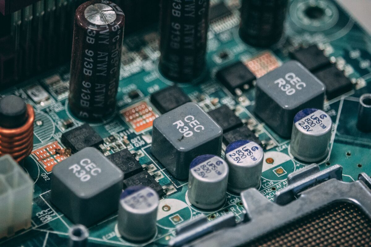
One of the most obvious advantages of advanced process technology is transistor density.
Imagine two chips:
3nm-generation design
┌────────────────────┐
│ █ █ █ █ █ █ █ █    │
│ █ █ █ █ █ █ █ █    │
│ █ █ █ █ █ █ █ █    │
└────────────────────┘

2nm-generation design
┌────────────────────┐
│ █ █ █ █ █ █ █ █ █  │
│ █ █ █ █ █ █ █ █ █  │
│ █ █ █ █ █ █ █ █ █  │
│ █ █ █ █ █ █ █ █ █  │
└────────────────────┘
This is only a conceptual illustration, but the idea is important.
Higher transistor density gives architects more options.
They can:
- add more processing resources
- increase cache capacity
- integrate more specialized accelerators
- reduce the area required for existing functionality
- improve performance within a similar physical footprint
TSMC’s published N2 research reports more than a 1.15× chip-density increase compared with its referenced 3nm technology, alongside performance or power improvements.
2nm and AI
AI is one of the major reasons advanced semiconductor technology matters so much right now.
Modern AI workloads involve enormous numbers of mathematical operations.
For example, neural networks repeatedly perform operations involving:
Matrix multiplication
        +
Vector operations
        +
Memory movement
        +
Activation functions
        +
Data transfers
AI processors therefore need huge computational throughput while keeping power consumption under control.
A more efficient process can allow chip designers to put more computational hardware into a given area or achieve similar performance at lower power.
This is important for both:
AI training
and
AI inference
Training large models requires enormous amounts of computation over long periods.
Inference happens whenever the trained model generates an answer, image, prediction, recommendation, or other output.
At massive scale, inference itself can consume substantial amounts of computing resources.
This is why semiconductor improvements are becoming directly connected to the economics of AI infrastructure.
2nm Could Matter Even More for Data Centers
The importance of power efficiency becomes much larger in a data center.
A single processor may consume hundreds of watts under heavy workloads.
A data center can contain thousands of processors.
So the calculation becomes:
Processor power
       ×
Number of processors
       ×
Hours of operation
       =
Large energy requirement
Reducing the energy required for each unit of computation can therefore have a system-level effect.
This is one reason advanced process technology is particularly relevant to high-performance computing and AI accelerators.
TSMC explicitly identifies N2 as a technology for both smartphones and high-performance computing applications.
2nm Is Not Just About Making CPUs Faster
It would be a mistake to think 2nm technology is mainly about increasing CPU clock speed.
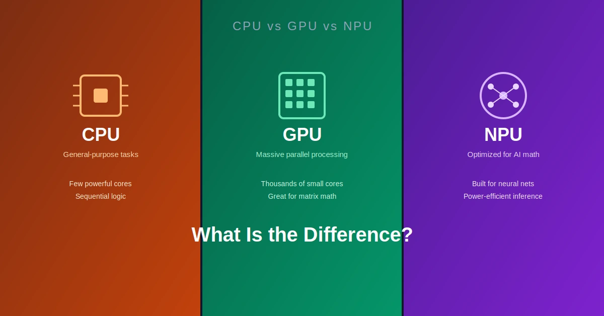
Modern processors are increasingly heterogeneous.
A single system-on-chip can contain:
CPU
 │
 ├── GPU
 │
 ├── NPU / AI accelerator
 │
 ├── Image processor
 │
 ├── Media engine
 │
 ├── Cache
 │
 ├── Security hardware
 │
 └── Connectivity components
The additional transistor budget can be used in different ways depending on the product.
A smartphone manufacturer may prioritize battery life and AI capabilities.
A server processor may prioritize compute throughput and cache.
An AI accelerator may prioritize matrix-processing hardware and memory bandwidth.
So the same manufacturing technology can support very different chip designs.
Why Smartphones Care About 2nm
Smartphones have a particularly difficult engineering constraint.
Users want:
- longer battery life
- faster applications
- better cameras
- on-device AI
- better graphics
- thinner devices
- less heat
All of these requirements compete for the same limited battery and thermal budget.
Suppose a future processor can perform a workload more efficiently.
The manufacturer has a choice:
Option A
Same performance → lower power

Option B
Same power → higher performance

Option C
Balance both → better battery life + more performance
This is why process technology improvements do not necessarily translate into a simple “X% faster phone.”
The manufacturer and chip designer decide how to use the available efficiency and transistor-density improvements.
The Importance of On-Device AI
One particularly interesting application is local AI.
Instead of sending every AI task to a cloud server, some workloads can run directly on a phone, PC, or other device.
For example:
Camera
   ↓
Local AI processor
   ↓
Image analysis
   ↓
Result
This can reduce latency and may improve privacy for some workloads because data does not necessarily need to leave the device.
However, running AI locally requires substantial computational capability while remaining within a small thermal and battery envelope.
More efficient semiconductor technology can therefore help make increasingly capable on-device AI practical.
2nm and Cache
Not every transistor in a processor is used for arithmetic.
A large amount of silicon can be dedicated to memory structures such as cache.
Cache is important because processors can perform calculations much faster than external memory can always supply data.
A simplified hierarchy looks like:
CPU/GPU
   ↓
L1 Cache
   ↓
L2 Cache
   ↓
L3 Cache
   ↓
DRAM
   ↓
Storage
More transistor density can give designers additional opportunities to integrate larger or more sophisticated on-chip memory structures.
TSMC’s N2 research has also demonstrated high-density SRAM technology alongside the logic process.
This matters because future processors are not only about adding more arithmetic units. Keeping those units supplied with data is equally important.
The Memory Problem Does Not Disappear
There is an important limitation here.
Making transistors smaller does not automatically solve every performance problem.
Modern processors increasingly encounter what engineers often call the memory wall.
The processor may be capable of performing calculations extremely quickly, but moving data between compute units and memory can become the limiting factor.
That is why modern AI systems increasingly depend on technologies such as:
- high-bandwidth memory
- advanced packaging
- large caches
- chiplets
- high-speed interconnects
- 3D integration
In other words:
Smaller transistors are only one part of modern computing.
2nm and Advanced Packaging
As transistor scaling becomes harder, the semiconductor industry is increasingly improving chips in another dimension: packaging.
Instead of putting everything into one enormous piece of silicon, designers can combine multiple components.
Conceptually:
┌──────────────┐
│ Compute Die  │
├──────────────┤
│ Compute Die  │
├──────────────┤
│ Memory       │
└──────────────┘
This can allow different technologies to be combined into a single system.
TSMC’s 2nm platform is also being developed alongside its 3D integration and advanced packaging technologies, reflecting the broader shift toward system-level scaling rather than relying only on transistor shrinking.
This is increasingly important for AI processors, where compute dies and high-bandwidth memory need to work together at extremely high data rates.
Why 2nm Manufacturing Is Difficult
Getting smaller transistors onto a chip is not simply a matter of using a smaller version of the same factory process.
Every process generation requires improvements throughout the manufacturing pipeline.
That includes:
- transistor architecture
- lithography
- materials
- deposition
- etching
- interconnects
- power delivery
- process control
- defect management
- yield
- chip design tools
A chip can theoretically have excellent transistor performance, but if manufacturing yield is poor, producing it economically becomes difficult.
Yield is particularly important.
If a wafer contains many defective dies, the cost of every usable chip increases.
That makes advanced-node manufacturing an enormous engineering and economic challenge.
Why 2nm Chips Are Expensive
Advanced semiconductor manufacturing requires extremely sophisticated fabrication facilities and equipment.
The cost does not stop at the fab itself.
Chip companies also need:
New process technology
        +
EDA software
        +
Process Design Kits
        +
IP libraries
        +
Verification
        +
Prototype wafers
        +
Testing
        +
Packaging
Designing a modern leading-edge chip can therefore cost enormous amounts of money before the first mass-produced processor reaches consumers.
This is one reason only a limited number of companies can compete at the leading edge of semiconductor manufacturing.
2nm Does Not Automatically Mean a Better Chip
This distinction is important.
A 2nm processor is not automatically better than every 3nm processor.
Actual performance depends on the complete design.
For example:
Process node
      +
Architecture
      +
Clock frequency
      +
Cache
      +
Memory bandwidth
      +
Power limits
      +
Software
      =
Real-world performance
A well-designed chip on an older process can outperform a poorly designed chip on a newer process for a particular workload.
The process technology provides a set of capabilities. The chip architecture determines how effectively those capabilities are used.
What Happens After 2nm?
2nm is not the end of transistor scaling.
Semiconductor companies are already working on technologies beyond the first generation of 2nm-class processes.
TSMC, for example, has described N2 extensions such as N2P and later technologies including A16 and A14. Its roadmap also shows continued movement toward nanosheet improvements and backside power delivery.
One interesting direction is backside power delivery.
Traditional chips generally route power and signals through the front side of the wafer.
A backside power architecture moves some power-delivery infrastructure to the back of the silicon.
Conceptually:
Front side
──────────────
Signal routing
Logic
──────────────
Silicon
──────────────
Back side
Power delivery
This can free valuable routing resources on the front side and improve power delivery.
TSMC’s A16 technology combines nanosheet transistors with its Super Power Rail approach and is designed for demanding HPC workloads.
This shows where the industry is heading: not simply “make the transistor smaller,” but redesign the entire way power, signals, memory, and compute are connected.
Will 2nm Make AI Much Faster?
Not by itself.
AI performance depends on many layers of the system.
For example:
Process technology
        ↓
Chip architecture
        ↓
Compute units
        ↓
Memory
        ↓
Interconnect
        ↓
Compiler / libraries
        ↓
AI framework
        ↓
Model
A 2nm process can provide better performance-per-watt and higher density, but the final AI performance depends on how the processor uses those improvements.
This distinction is important because semiconductor marketing can sometimes make a process node sound like a direct performance multiplier.
It isn’t.
The Bigger Picture: Computing Is Becoming More Energy-Constrained
The deeper reason 2nm matters is not simply transistor size.
It is the growing amount of computation society wants to perform.
AI models are getting larger.
Data centers are processing more workloads.
Smartphones are running increasingly sophisticated local AI.
PCs are adding dedicated AI accelerators.
Robotics and autonomous systems need continuous real-time computation.
All of this increases demand for computing power.
At the same time, electricity, cooling, battery capacity, and physical space remain limited.
That creates a fundamental engineering problem:
More computation
       ↓
More energy demand
       ↓
Need better efficiency
       ↓
Advanced semiconductor technology
2nm technology is one piece of that equation.
2nm Is a Step Toward the Next Computing Era
The significance of 2nm is therefore much broader than a smaller number printed on a semiconductor roadmap.
It represents another transition in transistor architecture and manufacturing technology.
The move toward nanosheet transistors is designed to maintain better control of extremely small transistor channels. Higher density provides designers with more transistor resources, while improved power efficiency can help control the energy cost of computation.
That combination matters for almost every major computing category:
Smartphones need more performance without sacrificing battery life.
AI accelerators need enormous computational throughput within practical power limits.
Data centers need more computing capacity without allowing electricity and cooling requirements to grow uncontrollably.
PCs need increasingly capable local AI processing.
High-performance computing systems need more performance per watt as workloads become more demanding.
Final Thoughts
The most important thing to understand about 2nm chips is that 2nm is not simply about making everything smaller.
The industry is changing transistor structures, improving density, reducing energy consumption, and redesigning how power and signals move through increasingly complex chips.
TSMC’s N2 technology is already in volume production, and the company is continuing to develop extensions and successor technologies.
The future of computing will not depend on transistor scaling alone. Advanced packaging, high-bandwidth memory, chiplets, specialized accelerators, software optimization, and new power-delivery technologies will all become increasingly important.
But transistor scaling remains one of the foundations.
As AI and other computational workloads continue to grow, the question is no longer simply how many calculations can a chip perform?
It is increasingly:
How much useful computation can we get from every square millimeter of silicon and every watt of electricity?
That is where technologies such as 2nm become important.
SiliconeUpdate.com is a technology news platform that publishes updates and informational content related to silicon technology, software, artificial intelligence, and emerging technologies.
All articles published on this platform are attributed to SiliconeUpdate.com instead of individual authors. Content is presented in a neutral, informational format without personal opinions.
—
Content Publishing
SiliconeUpdate.com publishes news and updates based on publicly available information, official announcements, and industry developments. The focus is on clarity, relevance, and timely reporting.
—
Editorial Control
All editorial decisions, updates, and content management are handled at the platform level. No individual human or AI identity is presented as the author of articles.
—
Contact
For editorial communication or general queries, contact:
Email: neemasharma@gmail.com