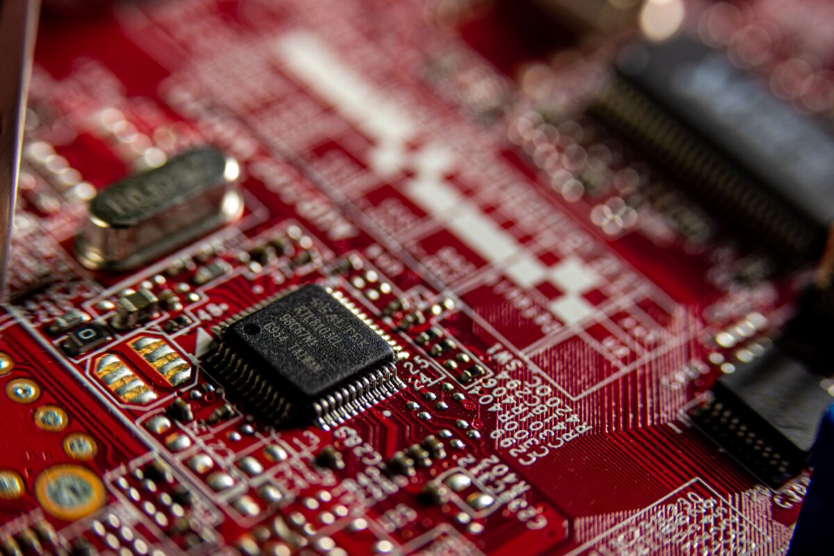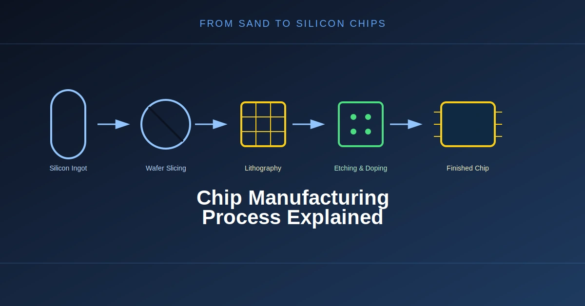
Chip manufacturing is the intricate process of converting circuit designs into functional semiconductor devices, commonly known as integrated circuits or microchips. This highly complex sequence involves hundreds of steps, transforming raw silicon into the sophisticated components that power modern electronics.
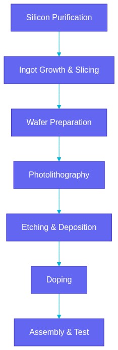
Foundries, specialized fabrication facilities, precisely execute these processes, which include photolithography, film deposition, and etching. The entire manufacturing journey, from initial silicon purification to final packaging and testing, demands extreme precision and a controlled environment.
Definition and Purpose
Chip manufacturing defines the fabrication of semiconductor devices on a silicon wafer, enabling the creation of transistors, resistors, and capacitors in microscopic arrangements. Its primary purpose is to realize complex digital and analog circuit designs into physical, high-performance components.
These chips serve as the fundamental building blocks for computing, communication, and control systems across virtually all industries. The process is critical for producing devices ranging from simple microcontrollers to advanced processors for generative AI, which are predicted to approach US$500 billion in revenue in 2026.
The Role of Foundries
Foundries are dedicated facilities equipped with the specialized machinery and expertise required for chip fabrication. They act as contract manufacturers, taking chip designs—the “architecture” laid out to achieve specific functions—and translating them into physical chips.
These facilities operate under stringent cleanroom conditions to prevent contamination, which can severely impact chip yield and performance. The capital investment and operational complexity of foundries are immense, reflecting the advanced nature of the manufacturing process.
The Foundation: Silicon Wafer Preparation
The journey of a semiconductor chip begins with silicon, a ubiquitous element refined to an ultra-pure state. This purified silicon forms the substrate upon which all subsequent circuit layers are built.
The quality of the initial silicon wafer directly impacts the performance and reliability of the final integrated circuit. Any impurities or structural defects introduced at this stage can propagate through the entire manufacturing process.
Silicon Purification
Raw silicon, typically derived from sand, undergoes a rigorous purification process to achieve semiconductor-grade purity, often exceeding 99.9999999% (9N purity). This involves chemical processes like the Siemens process, which converts metallurgical-grade silicon into trichlorosilane, then reduces it back to hyperpure polycrystalline silicon.
The resulting polysilicon is then melted in a crucible, preparing it for crystal growth. This extreme purity is essential because even trace impurities can alter the electrical properties of the semiconductor material.
Ingot Growth and Slicing
From the molten polysilicon, large, single-crystal silicon ingots are grown using methods like the Czochralski process. A small seed crystal is dipped into the melt and slowly pulled upwards while rotating, allowing a large, cylindrical single crystal to form.
These ingots, typically several feet long and up to 300mm in diameter, are then precisely sliced into thin wafers using diamond-edged saws. The wafers are subsequently polished to an atomic-level flatness and smoothness, creating the perfect surface for circuit fabrication.

Photo by SHOX ART on Pexels
Core Fabrication Steps
Once the silicon wafer is prepared, the intricate process of building the circuit layers begins. This involves a repetitive sequence of adding, patterning, and removing materials to create the desired electrical pathways and components.
Each layer adds complexity and functionality, requiring precise alignment and control over material properties. The accuracy of these steps determines the chip’s performance and its ability to function as designed.
Photolithography
Photolithography is the process of transferring a circuit pattern from a photomask onto the wafer surface. The wafer is coated with a light-sensitive material called photoresist, which is then exposed to ultraviolet (UV) light through the mask.
Areas of the photoresist exposed to light undergo a chemical change, allowing them to be selectively removed by a developer. This creates a precise pattern on the wafer, mirroring the design on the photomask, which defines where subsequent materials will be added or removed.
Etching and Deposition
Following photolithography, etching removes material from the wafer in the areas not protected by the photoresist. This can be done using wet chemical etchants or dry plasma etching, with dry etching offering finer control for smaller features.
Film deposition, conversely, adds thin layers of various materials—conductors, insulators, or semiconductors—onto the wafer. Techniques like Chemical Vapor Deposition (CVD) or Physical Vapor Deposition (PVD) are used to grow these films with precise thickness and composition.
Doping and Ion Implantation
Doping is the intentional introduction of impurities into the silicon crystal lattice to alter its electrical conductivity. This creates N-type (excess electrons) or P-type (electron holes) semiconductor regions, which are fundamental for forming transistors and diodes.
Ion implantation is a precise doping method where ions of dopant elements (e.g., boron, phosphorus) are accelerated and embedded into specific regions of the wafer. This technique offers superior control over the depth and concentration of dopants compared to diffusion methods.
Advanced Techniques and Equipment
The relentless demand for smaller, faster, and more powerful chips drives continuous innovation in manufacturing techniques. This necessitates increasingly sophisticated equipment and processes capable of handling features at the nanometer scale.
The complexity and cost of these advanced machines are significant, reflecting the cutting-edge science and engineering involved in their development.
Extreme Ultraviolet (EUV) Lithography
Extreme Ultraviolet (EUV) lithography represents a significant advancement in photolithography, utilizing light with a much shorter wavelength (13.5 nm) than traditional UV light. This allows for the patterning of extremely fine features, enabling the production of chips with smaller transistor sizes and higher densities.
EUV machines are among the most complex and expensive pieces of equipment in chip manufacturing, central to producing the most advanced processors. The technology’s development has been a central theme in the technical roadmap of chip manufacturing, with each generation becoming more intricate.
Metrology and Inspection
Throughout the manufacturing process, extensive metrology (measurement) and inspection steps are performed. These processes verify that each layer is correctly patterned, deposited, and etched according to design specifications.
Advanced optical and electron microscopy techniques are employed to detect defects, measure critical dimensions, and ensure proper material composition. Early detection of anomalies prevents costly errors in later stages and maintains high yield rates.
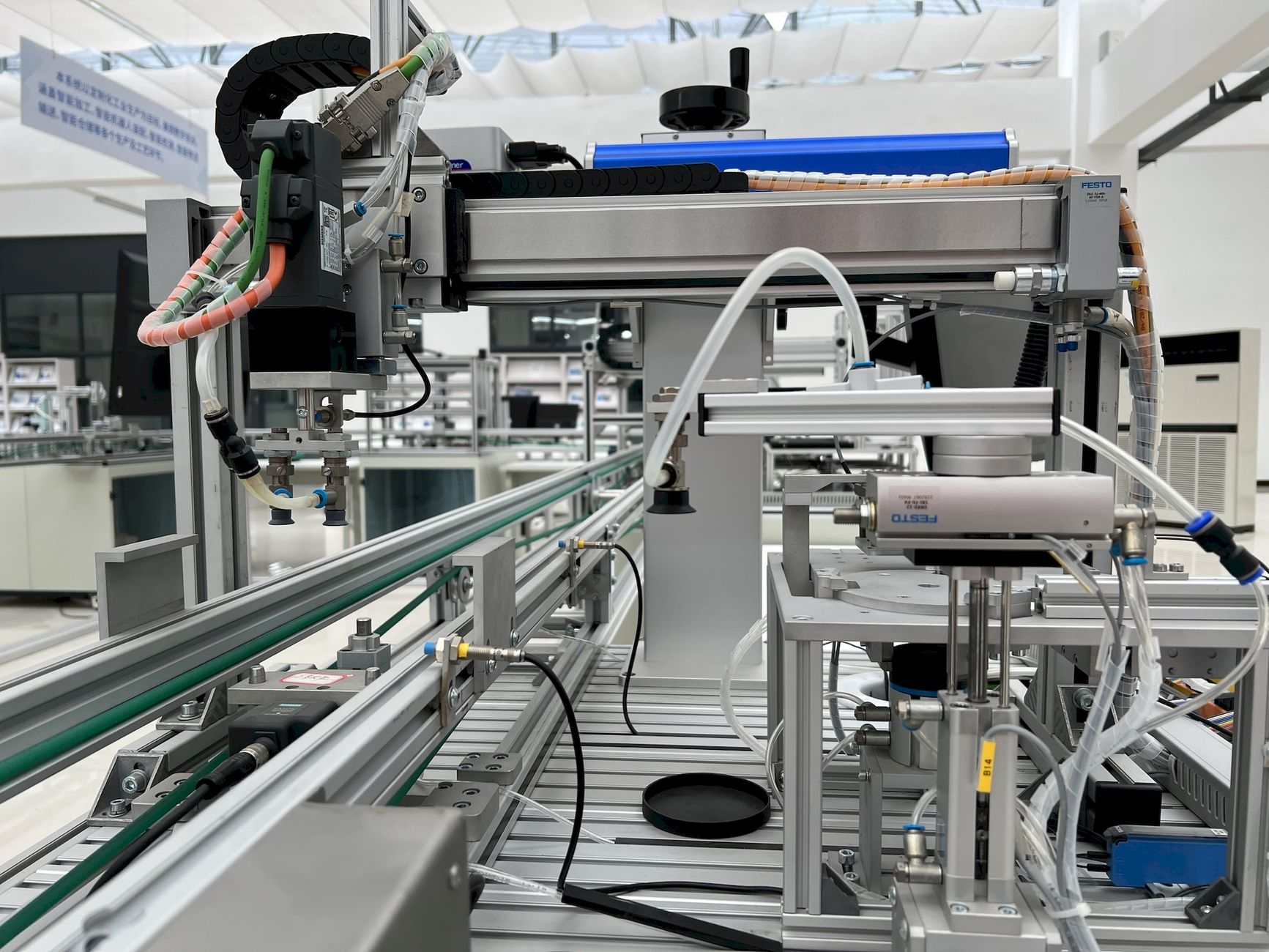
Photo by KJ Brix on Pexels
Assembly, Testing, and Packaging
After the fabrication of circuits on the wafer is complete, the individual chips must be separated, tested, and prepared for integration into electronic devices. This final stage ensures that only functional chips reach the market.
These steps are crucial for protecting the delicate semiconductor dies and providing reliable electrical connections to external components.
Wafer Dicing and Die Bonding
Once all fabrication steps on the wafer are finished, the wafer contains hundreds or thousands of individual chips, or “dies.” Wafer dicing is the process of cutting the wafer into these individual dies using a high-precision saw.
Each functional die is then picked and attached to a lead frame or substrate in a process called die bonding. This typically involves an adhesive or solder, creating the initial physical connection for the chip.
Packaging and Final Test
The bonded die is then encapsulated in a protective package, which provides mechanical support, environmental protection, and a means for electrical connection to a circuit board. Various packaging types exist, such as Ball Grid Array (BGA) or Quad Flat Package (QFP), depending on the application.
Finally, each packaged chip undergoes a rigorous final test to verify its electrical functionality, performance, and reliability under various operating conditions. Only chips that pass all tests are shipped to customers, ensuring quality and adherence to specifications.
Key Manufacturing Process Stages
The table below outlines the primary stages of the chip manufacturing process, detailing their core functions and typical materials involved.
| Stage | Primary Function | Key Materials/Equipment |
|---|---|---|
| Wafer Preparation | Create ultra-pure, flat silicon substrate | Polysilicon, Czochralski furnace, Diamond saws |
| Photolithography | Pattern circuit designs onto wafer | Photoresist, Photomasks, UV/EUV scanners |
| Etching | Remove unwanted material | Plasma etchers, Wet chemical baths |
| Deposition | Add thin layers of material | CVD/PVD reactors, Various gases/metals |
| Doping | Alter silicon conductivity | Ion implanters, Dopant gases (e.g., Boron, Phosphorus) |
| Assembly & Test | Separate, package, and verify chips | Wafer saws, Die bonders, Test equipment, Packaging materials |
Key Takeaways
- Chip manufacturing transforms raw silicon into functional integrated circuits through a multi-stage process.
- The process begins with silicon purification and wafer preparation, establishing a pristine substrate.
- Core fabrication involves repetitive cycles of photolithography, etching, deposition, and doping to build circuit layers.
- Advanced techniques like EUV lithography are essential for creating the nanometer-scale features of modern chips.
- The final stages include wafer dicing, die bonding, packaging, and rigorous testing to ensure chip functionality and reliability.
The extreme precision required in chip manufacturing means that even a single dust particle, invisible to the naked eye, can render a multi-million dollar wafer useless. This necessitates operating in environments significantly cleaner than a hospital operating room.
Global Semiconductor Market Segments (2025-2026)
Total Sales (2025): 790Billion USD | Generative AI Chips (2026): 500Billion USD — Source: Moody’s 2026, Deloitte 2026
Real World Example
Consider the manufacturing of a modern smartphone processor, a system-on-a-chip (SoC) that integrates CPU, GPU, memory controllers, and other components. The design for such a chip, developed by companies like Apple or Qualcomm, is sent to a foundry such as TSMC or Samsung.
The foundry then takes a 300mm silicon wafer and begins the fabrication. Hundreds of layers are built up, each requiring a cycle of cleaning, film deposition, photolithography using advanced EUV scanners, etching, and ion implantation. For instance, creating the billions of transistors on a single processor might involve over 1,000 individual process steps.
After fabrication, the wafer is diced into individual processor dies. Each die is then mounted onto a substrate, wire-bonded, and encapsulated in a protective package. Finally, extensive electrical tests are performed on every single packaged chip to ensure it meets the stringent performance and power consumption specifications required for a smartphone, before being shipped to the device manufacturer.
Frequently Asked Questions
What is the primary material used in chip manufacturing?
The primary material is highly purified silicon, which serves as the semiconductor substrate. This silicon is refined to an extremely high purity level before being grown into single-crystal ingots and sliced into wafers.
Why is a “cleanroom” environment essential for chip manufacturing?
A cleanroom environment is essential to prevent contamination by microscopic particles. Even tiny dust particles can cause defects on the nanometer-scale features of a chip, leading to malfunctions or complete failure.
What is the significance of photolithography in the process?
Photolithography is significant because it transfers the intricate circuit patterns from a design mask onto the silicon wafer. This step dictates the precise geometry and arrangement of all components on the chip.
How has chip manufacturing evolved to meet demand for smaller chips?
Chip manufacturing has evolved through advancements like Extreme Ultraviolet (EUV) lithography, which uses shorter wavelengths of light to pattern finer features. This allows for the creation of smaller transistors and denser integrated circuits, enabling more powerful and efficient chips.

SiliconeUpdate.com is a technology news platform that publishes updates and informational content related to silicon technology, software, artificial intelligence, and emerging technologies.
All articles published on this platform are attributed to SiliconeUpdate.com instead of individual authors. Content is presented in a neutral, informational format without personal opinions.
—
Content Publishing
SiliconeUpdate.com publishes news and updates based on publicly available information, official announcements, and industry developments. The focus is on clarity, relevance, and timely reporting.
—
Editorial Control
All editorial decisions, updates, and content management are handled at the platform level. No individual human or AI identity is presented as the author of articles.
—
Contact
For editorial communication or general queries, contact:
Email: neemasharma@gmail.com