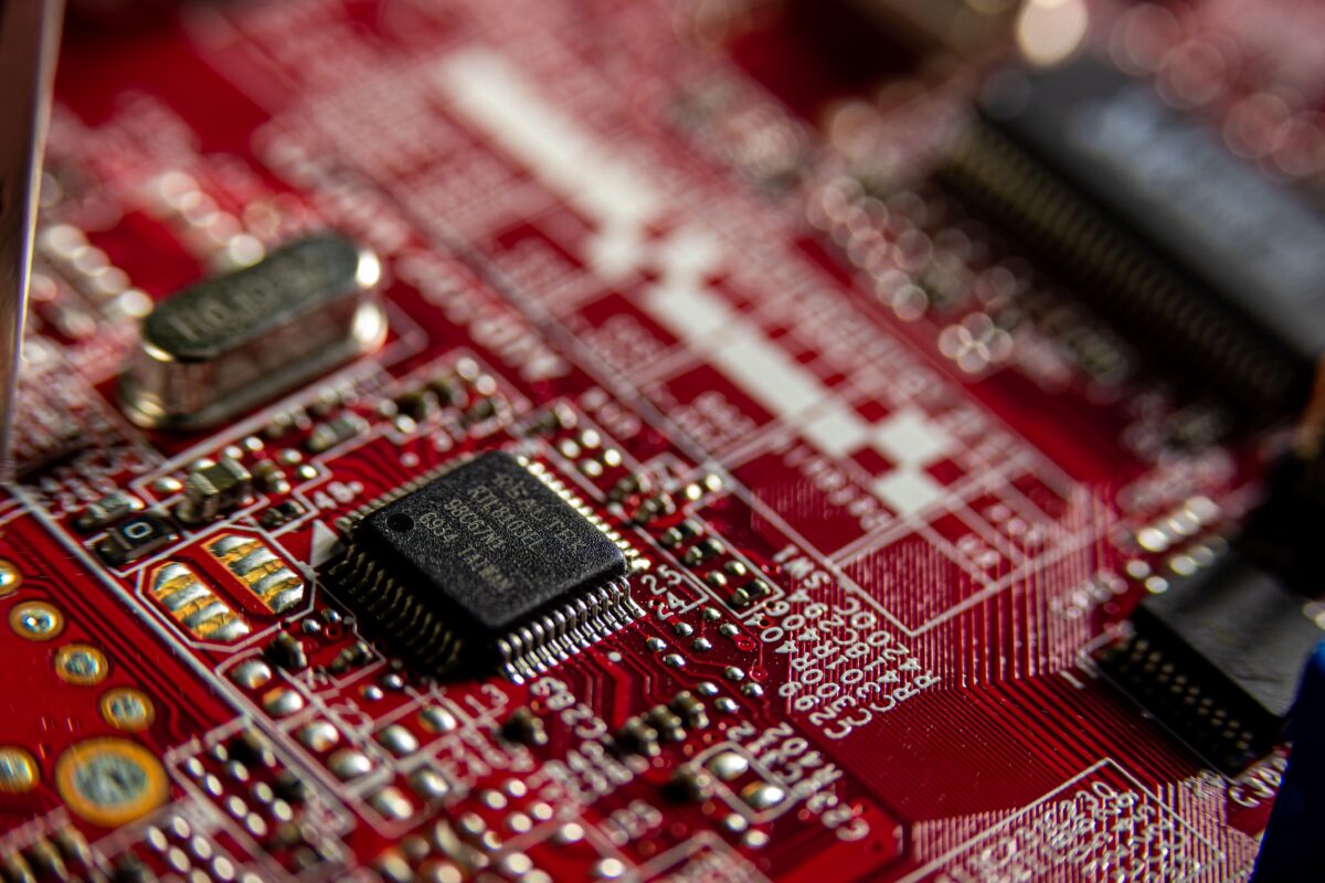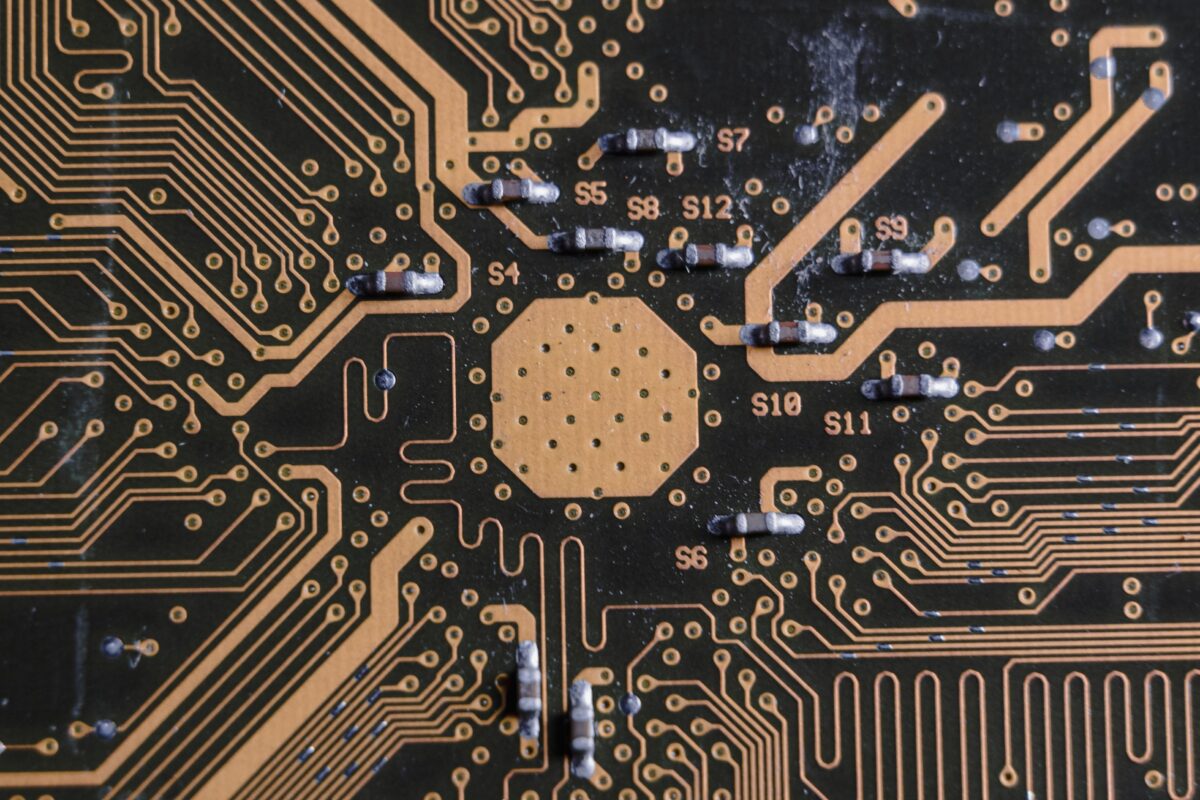
Photolithography is a fundamental process in semiconductor manufacturing, essential for printing intricate patterns onto silicon wafers. This technique enables the creation of microscopic features, shaping every transistor and interconnection on a chip with extreme precision.
The process involves guiding light patterns through a designed mask to define microstructures. These patterns are critical for the functionality of integrated circuits, dictating the layout and connectivity of millions or billions of transistors.
The Core Principle of Pattern Transfer
At its heart, photolithography operates by transferring a geometric pattern from a photomask to a light-sensitive chemical layer, known as photoresist, on the wafer surface. This is analogous to exposing a photograph, where light selectively alters the chemical properties of the photoresist.
The patterned photoresist then acts as a protective layer or a stencil for subsequent etching or deposition steps, allowing the underlying silicon to be selectively modified according to the desired circuit design.
The Fundamental Process of Photolithography
The photolithography process involves several sequential steps to accurately transfer circuit designs onto a semiconductor wafer. Each step requires precise control to achieve the nanometer-scale features demanded by modern chip manufacturing.
Wafer Preparation and Photoresist Application
Before pattern transfer, silicon wafers undergo thorough cleaning to remove contaminants. A uniform layer of photoresist, a light-sensitive polymer, is then applied to the wafer surface, typically by spin-coating. The thickness and uniformity of this layer are critical for pattern fidelity.
This photoresist layer is then pre-baked to remove solvents and improve adhesion, preparing it for exposure to light.
Exposure and Pattern Transfer
The prepared wafer is then placed into a lithography system, where it is exposed to light through a photomask (also called a reticle or stencil). The photomask contains the desired circuit pattern. Light passes through the transparent areas of the mask and is blocked by the opaque areas, projecting the pattern onto the photoresist.
The light causes a chemical change in the exposed areas of the photoresist. For positive photoresists, exposed areas become soluble; for negative photoresists, exposed areas become insoluble.
Development and Pattern Definition
After exposure, the wafer is subjected to a chemical developer solution. This solution selectively removes either the exposed or unexposed photoresist, depending on the type of photoresist used. The remaining photoresist forms a precise replica of the pattern from the photomask.
This patterned photoresist layer then serves as a protective barrier for subsequent processing steps, such as etching, ion implantation, or material deposition, which permanently transfer the pattern into the underlying wafer material.
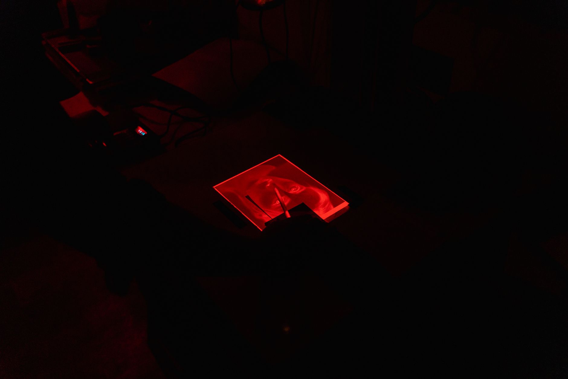
Photo by Tima Miroshnichenko on Pexels
Key Lithography Technologies: DUV and EUV
The semiconductor industry employs different lithography technologies, primarily distinguished by the wavelength of light used. The choice of technology directly impacts the minimum feature size that can be printed and, consequently, the density and performance of integrated circuits.
Deep Ultraviolet (DUV) Lithography
DUV lithography systems utilize deep-ultraviolet light to transfer circuit patterns from a photomask onto semiconductor wafers. This technology has been a workhorse for many generations of chip manufacturing, enabling feature sizes down to tens of nanometers.
DUV systems are robust and widely adopted, but their ability to print increasingly smaller features is limited by the wavelength of light they employ.
Extreme Ultraviolet (EUV) Lithography
EUV lithography represents the cutting edge of pattern printing, using extreme ultraviolet light to project patterns onto silicon wafers. This technology is essential for manufacturing leading-edge chips, allowing for the creation of features at the single-digit nanometer scale.
ASML’s EUV lithography machines are central to this advancement, enabling the intricate, microscopic stencil patterns required to connect billions of transistors on advanced chips, layer by layer. ASML’s EUV technology is critical for modern chip fabrication.
EUV Lithography Advancements and Impact
Continuous innovation in EUV lithography is vital for meeting the escalating demands of the semiconductor industry for smaller, more powerful, and more energy-efficient chips.
Increasing Light Source Power
A significant advancement in EUV technology involves increasing the power of the extreme ultraviolet light source. As of February 2026, ASML has boosted its EUV light source power to 1000 watts. This higher light source power directly translates to shorter exposure times for the photoresist.
The increased power allows for faster processing of wafers, which is crucial for high-volume manufacturing.
Impact on Chip Production Capacity
The upgrade to a 1000-watt EUV light source is projected to significantly enhance chip production capabilities. By 2030, this advancement could enable a 50% increase in the output of chips from EUV machines. This boost in throughput is critical for meeting the global demand for advanced semiconductors.
The ability to produce more chips faster directly impacts the cost and availability of leading-edge electronic devices.

Photo by Nicolas Foster on Pexels
The Significance of Photolithography
Photolithography is not merely a manufacturing step; it is the cornerstone that enables the very existence of modern electronics. Its precision dictates the capabilities of every digital device.
Enabling Microscopic Circuitry
The process prints patterns onto silicon wafers with near-impossible precision, shaping every transistor. Without this capability, the miniaturization and integration of billions of transistors onto a single chip would be impossible.
Photolithography defines the microstructures that form the intricate networks of transistors and interconnects, allowing complex functionalities within a tiny footprint.
Foundation for Advanced Chips
To connect the vast number of transistors on advanced chips, chipmakers rely on EUV photolithography systems to print microscopic stencil patterns. This is done one layer at a time, building up the complex three-dimensional structures of modern integrated circuits. The layer-by-layer patterning is fundamental to chip design.
The precision and capability of photolithography directly correlate with the performance, power efficiency, and cost-effectiveness of contemporary semiconductor devices.
Comparison of Lithography Technologies
| Feature | DUV Lithography | EUV Lithography |
|---|---|---|
| Light Source Wavelength | Deep Ultraviolet (e.g., 193 nm) | Extreme Ultraviolet (13.5 nm) |
| Typical Feature Size | Tens of nanometers | Single-digit nanometers |
| Application | Mature process nodes, less critical layers | Leading-edge chip manufacturing |
| Complexity | High | Extremely High (e.g., vacuum environment, complex optics) |
| Light Source Power (2026) | Not specified in data for DUV | Up to 1000 Watts (ASML) |
Key Takeaways
- Photolithography is the process of printing intricate circuit patterns onto silicon wafers, forming transistors and interconnections.
- The process involves applying photoresist, exposing it to light through a photomask, and then developing the pattern.
- DUV lithography uses deep-ultraviolet light for pattern transfer, while EUV lithography employs extreme ultraviolet light for leading-edge chips.
- ASML’s EUV machines are critical for advanced chip manufacturing, projecting patterns with high precision.
- Recent advancements include boosting EUV light source power to 1000 watts, potentially increasing chip output by 50% by 2030.
The ability of photolithography to precisely define patterns at the atomic scale is not just an engineering feat; it underpins the entire digital revolution, making possible devices that were once considered science fiction.
Real World Example
Consider the manufacturing of a high-performance processor for a modern smartphone. This processor contains billions of transistors, each needing to be precisely placed and connected. The fabrication begins with a blank silicon wafer.
An EUV photolithography system is employed to print the initial layer’s microscopic patterns onto the wafer. A thin layer of photoresist is applied, and then the EUV light projects the circuit design from a photomask onto this layer. After development, the patterned photoresist acts as a stencil. Subsequent etching steps remove material from the wafer where the photoresist is absent, creating the first set of transistor gates and interconnects.
This process is repeated dozens of times, with each layer requiring a new photolithography step to print its specific pattern. Each layer builds upon the previous one, gradually forming the complex three-dimensional structure of the processor. The precision of EUV lithography ensures that these layers align perfectly, enabling the intricate connections necessary for the chip’s functionality.
Frequently Asked Questions
What is the primary purpose of photolithography in chip manufacturing?
Photolithography’s primary purpose is to print intricate circuit patterns onto silicon wafers with extreme precision. These patterns define the transistors and interconnections that form integrated circuits.
How does photoresist contribute to the photolithography process?
Photoresist is a light-sensitive chemical layer applied to the wafer. When exposed to light through a mask, its chemical properties change, allowing selective removal during development to create the desired pattern.
What is the difference between DUV and EUV lithography?
DUV lithography uses deep-ultraviolet light and is suitable for mature process nodes, while EUV lithography uses extreme ultraviolet light to achieve the single-digit nanometer features required for leading-edge chips.
How do advancements in EUV light source power impact chip production?
Increasing EUV light source power, such as ASML’s 1000-watt source, shortens exposure times and increases wafer throughput. This can lead to a significant boost in chip production capacity, potentially by 50% by 2030.
SiliconeUpdate.com is a technology news platform that publishes updates and informational content related to silicon technology, software, artificial intelligence, and emerging technologies.
All articles published on this platform are attributed to SiliconeUpdate.com instead of individual authors. Content is presented in a neutral, informational format without personal opinions.
—
Content Publishing
SiliconeUpdate.com publishes news and updates based on publicly available information, official announcements, and industry developments. The focus is on clarity, relevance, and timely reporting.
—
Editorial Control
All editorial decisions, updates, and content management are handled at the platform level. No individual human or AI identity is presented as the author of articles.
—
Contact
For editorial communication or general queries, contact:
Email: neemasharma@gmail.com