Almost every modern electronic device depends on semiconductors.
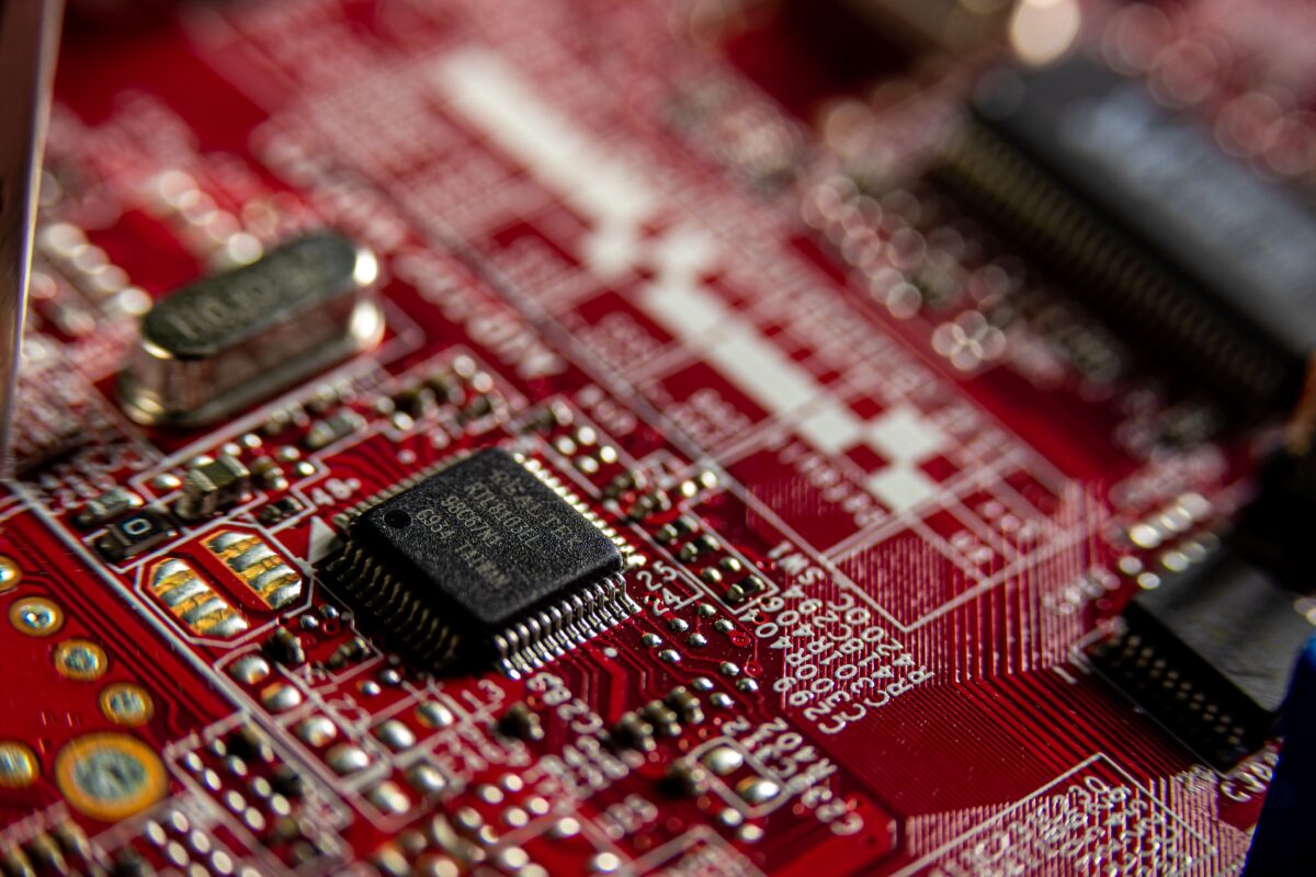
Your smartphone, laptop, car, Wi-Fi router, data center, graphics card, AI accelerator and even many household appliances contain semiconductor devices. The processors inside these systems may look like small pieces of silicon, but billions of microscopic electronic components can be built into a single chip.
At the center of all of this is a simple idea:
A semiconductor is a material whose electrical behavior can be controlled.
That ability to control the movement of electrical charge is what allows engineers to build transistors, diodes, memory cells, sensors and integrated circuits.
Silicon is the most widely used semiconductor material, although it is not the only one. Other semiconductor materials include gallium nitride (GaN), gallium arsenide (GaAs) and silicon carbide (SiC), which are useful for different applications.
So how does a material become a computer chip?
The answer starts at the atomic level.
What Is a Semiconductor?
A semiconductor is a material whose electrical conductivity falls between that of a good conductor and an insulator, and whose conductivity can be deliberately changed through factors such as impurities, electric fields, temperature and light.
IBM describes semiconductors as materials that can behave more like conductors or insulators depending on conditions. This controllability is what makes them useful for electronic devices.
A simple comparison is:
Conductor             Semiconductor             Insulator

Copper                Silicon                   Glass
Aluminum              Germanium                 Rubber

Current flows         Current can be             Current is
easily                controlled                 strongly resisted
Copper is useful when we want electricity to flow with relatively low resistance.
Glass is useful when we want to prevent current from flowing.
A semiconductor is useful when we want to control whether and how electricity flows.
That last property is the key.
A semiconductor is not simply a material that conducts “half as well” as copper. Its real value comes from the fact that engineers can manipulate its electrical properties.
Why Silicon Is Used in Computer Chips
Silicon is the dominant material used for many modern integrated circuits.
There are several reasons for this.
Silicon is relatively abundant, forms a stable crystal structure, and can be processed into extremely pure wafers. It also forms silicon dioxide, an insulating material that has been extremely important in the development of silicon-based transistor technology.
IBM notes that silicon’s abundance, stability and useful material properties helped make it a practical foundation for transistor manufacturing.
The basic path looks like this:
Silicon source
     ↓
Highly purified silicon
     ↓
Single-crystal silicon
     ↓
Silicon ingot
     ↓
Thin wafer
     ↓
Transistors
     ↓
Integrated circuit
     ↓
Packaged chip
The material therefore goes through a remarkable transformation.
The silicon itself is not a CPU.
The CPU is created by carefully modifying the silicon and building microscopic structures on top of it.
Silicon at the Atomic Level
To understand why silicon works, it helps to look at its atoms.
A silicon atom has four valence electrons.
In a silicon crystal, silicon atoms form bonds with neighboring atoms.
A simplified representation looks like:
        Si
       /  \
     Si -- Si
       \  /
        Si
In a pure silicon crystal, the electrons are strongly involved in these bonds.
At very low temperatures, pure silicon does not behave like a highly conductive metal.
But silicon has an important property: its electrical behavior can be modified.
This is where doping becomes important.
What Is Doping?

Doping is the intentional introduction of very small amounts of other elements into a semiconductor to change its electrical properties.
It may sound like contamination, but in semiconductor manufacturing it is a highly controlled engineering process.
IBM describes two fundamental forms:
- N-type doping
- P-type doping
The purpose is to change the number and type of charge carriers available inside the semiconductor.
N-Type Semiconductor
For N-type silicon, engineers introduce an element with more valence electrons than silicon.
Phosphorus is a common example.
Silicon has four valence electrons.
Phosphorus has five.
When phosphorus replaces a silicon atom in the crystal structure, four of its electrons can participate in bonding while one is more weakly bound.
That additional electron can become a mobile charge carrier.
Conceptually:
Silicon crystal
      +
Dopant with extra electron
      ↓
More available electrons
      ↓
N-type semiconductor
The “N” refers to the negative charge carriers associated with electrons.
P-Type Semiconductor
P-type doping works differently.
A dopant such as boron has fewer valence electrons than silicon.
This creates an absence of an electron in the crystal’s bonding structure.
That absence is treated as a hole.
A hole is not a physical particle in the same sense as an electron. It represents an available state that behaves like a positive charge carrier in semiconductor physics.
Conceptually:
Silicon crystal
      +
Dopant with fewer electrons
      ↓
Electron deficiency
      ↓
Hole
      ↓
P-type semiconductor
The “P” refers to the positive charge-carrier behavior associated with holes.
Why P-Type and N-Type Materials Matter
The real power of semiconductor engineering appears when different regions of semiconductor material are placed next to each other.
For example:
P-type silicon | N-type silicon
This creates a P-N junction.
P-N junctions are fundamental to many semiconductor devices, including diodes and transistors.
When the two regions meet, charge carriers move and redistribute near the boundary. This creates a region called the depletion region, where mobile charge carriers are greatly reduced.
The resulting electrical behavior can be controlled by applying voltage.
This is one of the basic physical principles behind semiconductor electronics.
What Is a Transistor?
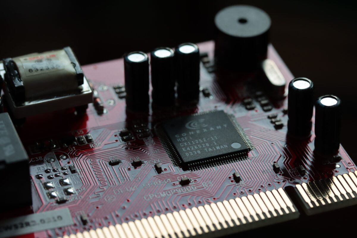
The transistor is arguably the most important semiconductor device in modern computing.
At a basic level, a transistor can act as a controllable electronic switch.
Intel describes modern computer chips as massive collections of microscopic transistors.
A simplified transistor concept is:
                 Gate
                  │
                  ▼
              ┌───────┐
Source ───────┤Channel├─────── Drain
              └───────┘
The gate controls what happens in the channel between the source and drain.
When the transistor is switched on, current can flow through the channel.
When it is switched off, the channel prevents normal current flow.
This gives digital electronics something extremely useful:
ON  →  1
OFF →  0
A computer can combine enormous numbers of these switches to represent and manipulate binary information.
How a MOSFET Works
Most modern digital logic is built using MOSFET-based transistor technology.
MOSFET stands for:
Metal-Oxide-Semiconductor Field-Effect Transistor
A simplified MOSFET has three important terminals:
          Gate
           │
           ▼
       ┌────────┐
       │        │
Source ─┤Channel├─ Drain
       │        │
       └────────┘
The gate does not simply act like a mechanical button.
Instead, applying an appropriate voltage to the gate creates an electric field that changes the conductivity of the region underneath it.
For an n-channel MOSFET, applying the appropriate gate voltage can create a conducting channel between source and drain.
Remove that voltage and the channel disappears or becomes sufficiently non-conductive for the intended operation.
Intel’s explanation of modern MOSFETs describes the source, drain, channel and gate relationship and how gate voltage controls current through the channel.
This is where the semiconductor’s controllable electrical properties become a practical switch.
From Transistors to Logic Gates
A single transistor is useful, but computers need much more than individual switches.
Transistors are connected together to create logic gates.
Some fundamental logic gates are:
AND
OR
NOT
For example, an AND gate produces an output of 1 only when both inputs are 1.
A   B   Output

0   0     0
0   1     0
1   0     0
1   1     1
These simple operations can be combined to create increasingly complicated circuits.
The hierarchy looks roughly like:
Transistors
     ↓
Logic gates
     ↓
Digital circuits
     ↓
Functional units
     ↓
Processor
     ↓
Computer system
Intel describes this progression from individual transistors to logic gates, circuits and processors.
A modern processor is therefore not a mysterious object that somehow “understands” instructions directly.
At the hardware level, it is an enormous network of electrical components performing controlled operations.
How Do Billions of Transistors Fit on a Chip?
This is where semiconductor manufacturing becomes extremely sophisticated.
Engineers do not manually place billions of transistors onto a piece of silicon.
Instead, chip designs are transferred onto silicon wafers using highly precise manufacturing processes.
A simplified process looks like:
Chip design
    ↓
Photomasks
    ↓
Silicon wafer
    ↓
Patterning
    ↓
Deposition
    ↓
Etching
    ↓
Doping / implantation
    ↓
Interconnects
    ↓
Repeated layers
    ↓
Finished wafer
Modern semiconductor fabrication repeats different processes many times to create transistor structures and the interconnect layers that connect them.
What Is a Silicon Wafer?
A wafer is a thin, circular piece of highly purified semiconductor material.
For mainstream silicon manufacturing, large wafers are processed to create many copies of integrated circuits at once.
Intel’s current terminology guide describes wafers as circular slices of ultra-pure silicon from which multiple dies are fabricated.
A simplified view is:
        Silicon wafer

       _______________
     /                 \
    /   □ □ □ □ □ □    \
   |   □ □ □ □ □ □ □    |
   |   □ □ □ □ □ □ □    |
    \   □ □ □ □ □ □    /
     \_________________/

          ↓

       Individual dies
Each small rectangular section can eventually become an individual chip die.
What Is a Die?
A die is an individual piece of semiconductor containing the integrated circuit.
The wafer contains many dies.
After fabrication and testing, the wafer is cut into individual pieces.
The process is roughly:
Large wafer
    ↓
Many circuit dies
    ↓
Wafer cutting
    ↓
Individual dies
    ↓
Packaging
    ↓
Finished chips
The terms “die” and “chip” are sometimes used interchangeably in casual conversation, but technically they are not always the same thing.
A die is the semiconductor piece containing the circuit.
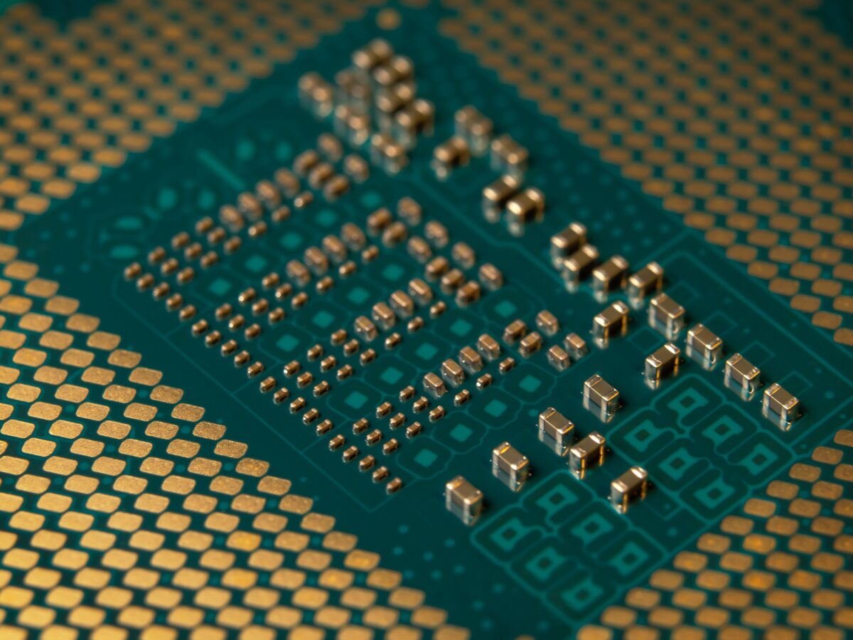
A packaged chip includes the die plus the package and connections that allow it to be mounted and electrically connected to a system.
How Are Transistors Printed Onto Silicon?
One of the critical processes is photolithography.
The basic idea is surprisingly similar to using a stencil.
A pattern is transferred onto the wafer using light and a mask.
Conceptually:
Light
  ↓
Mask
  ↓
Lens
  ↓
Pattern
  ↓
Silicon wafer
The process is repeated for different layers.
After patterning, materials can be deposited or removed using processes such as etching.
IBM describes wafer fabrication as involving processes including oxidation, masking/photolithography, etching and doping.
Modern fabs use extremely advanced versions of these techniques to create structures at nanometer-scale dimensions.
What Does “2nm” or “3nm” Mean?
This is where semiconductor terminology becomes confusing.
When you hear:
3nm chip
2nm chip
it does not necessarily mean that every transistor feature on the chip is exactly 3 or 2 nanometers wide.
Modern process-node names are better understood as identifiers for generations of semiconductor manufacturing technology rather than a single physical measurement.
The process involves a collection of design rules, transistor structures, materials and manufacturing technologies.
Intel’s current explanation of chip terminology also distinguishes process nodes from the physical dimensions of an individual chip.
As semiconductor technology advances, manufacturers attempt to improve combinations of:
- transistor density
- performance
- power efficiency
- manufacturing cost
- reliability
These trade-offs are collectively important to chip design.
Why Smaller Transistors Matter
A smaller transistor can potentially allow more transistors to be placed in a given area.
More transistors can provide additional circuitry and capabilities.
The basic idea is:
Older technology
┌───────────────┐
│  transistor   │
│  transistor   │
│  transistor   │
└───────────────┘

Newer technology
┌───────────────┐
│███████████████│
│███████████████│
│███████████████│
│███████████████│
└───────────────┘
The real situation is far more complicated, but increasing transistor density has historically been one of the major drivers of computing progress.
This is closely associated with Moore’s Law, Gordon Moore’s observation about the growth in transistor density over time.
However, modern semiconductor progress is not simply about making everything smaller.
Engineers also have to deal with:
- heat
- power consumption
- leakage
- manufacturing variability
- interconnect delays
- fabrication cost
- design complexity
Semiconductors Are Not Only CPUs
When people hear “semiconductor,” they often immediately think of a CPU.
But semiconductor technology covers a much broader range of devices.
Examples include:
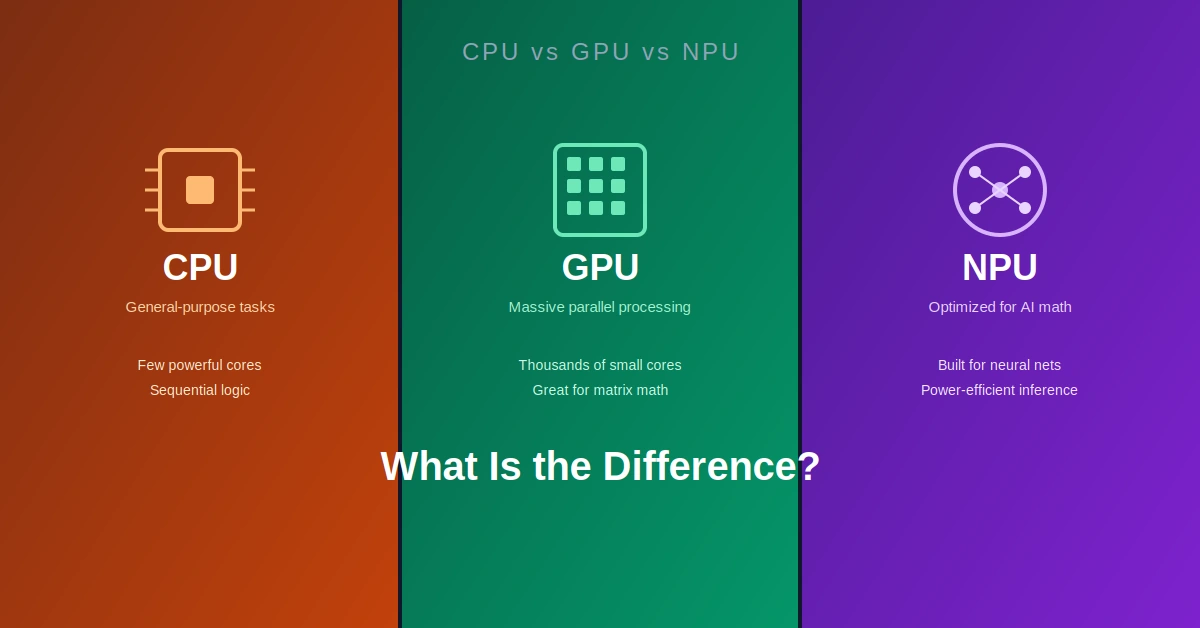
CPUs
Central processing units execute general-purpose instructions.
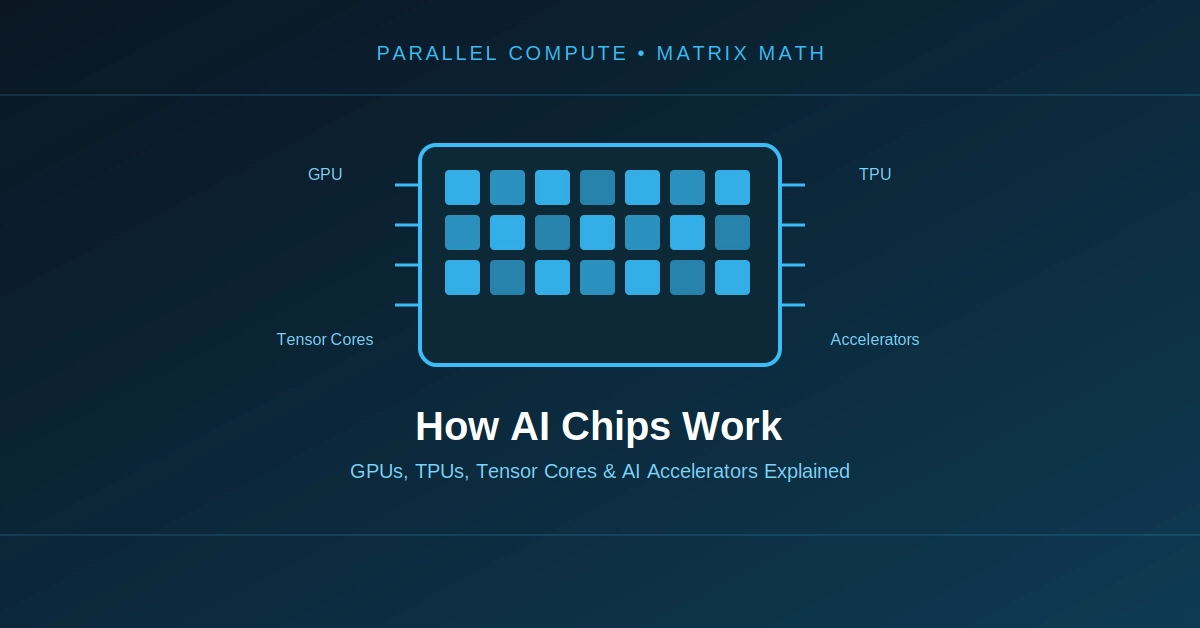
GPUs
Graphics processing units contain large numbers of processing resources designed for highly parallel workloads.
They are now also heavily used for AI and scientific computing.
Memory
Semiconductor memory includes technologies such as DRAM, SRAM and flash memory.
Microcontrollers
Microcontrollers combine processing, memory and peripheral functionality for embedded systems.
They can be found in vehicles, appliances, industrial equipment and countless other devices.
Power Semiconductors
Power semiconductor devices are designed to control electrical power.
Technologies such as silicon carbide and gallium nitride can be useful in applications involving high voltage, high frequency or high efficiency.
Sensors
Semiconductor devices can also detect physical conditions such as light, temperature, pressure and motion.
So “semiconductor” is not synonymous with “processor.”
It is a much broader category of electronic technology.
Silicon Is Not the Only Semiconductor
Silicon dominates mainstream logic manufacturing, but other materials are important in specific applications.
Examples include:
Silicon (Si)
Gallium Nitride (GaN)
Gallium Arsenide (GaAs)
Silicon Carbide (SiC)
Germanium (Ge)
Different materials have different electrical and physical characteristics.
For example, GaN and SiC are important in power electronics, while GaAs has long been useful in certain high-frequency and optoelectronic applications.
This is why the semiconductor industry is not simply a “silicon industry.”
Silicon remains fundamental, but different semiconductor materials serve different engineering requirements.
Why Semiconductors Are So Important to AI
Artificial intelligence has made semiconductor technology even more important.
Large AI models require enormous amounts of computation.
That computation is performed by specialized hardware containing huge numbers of transistors.
A modern AI accelerator can contain billions of transistors arranged into processing units, memory interfaces, caches, interconnects and other specialized circuitry.
The relationship can be simplified as:
Semiconductor
      ↓
Transistors
      ↓
Logic circuits
      ↓
Processing units
      ↓
AI accelerator
      ↓
AI computation
This is why AI development and semiconductor development are increasingly connected.
Better semiconductor technology can provide improvements in computing performance, energy efficiency and memory bandwidth, which are all important for AI workloads.
From Electricity to Computation
The most interesting part of semiconductor technology is how something physical becomes computation.
At the lowest level:
Voltage
   ↓
Electric field
   ↓
Semiconductor behavior
   ↓
Transistor switching
   ↓
Logic gates
   ↓
Digital circuits
   ↓
Binary operations
   ↓
Software execution
A CPU instruction such as an addition looks very abstract from the programmer’s perspective.
At the hardware level, however, that operation eventually becomes electrical activity moving through carefully designed transistor networks.
The software is abstract.
The hardware underneath it is physical.
Semiconductors provide the controllable electrical behavior that connects those two worlds.
Why Semiconductor Manufacturing Is So Difficult
Designing a chip is only one part of the semiconductor industry.
Manufacturing it reliably is another enormous challenge.
A modern fabrication facility needs:
- extremely clean environments
- highly purified materials
- advanced lithography equipment
- precise deposition systems
- etching equipment
- ion implantation systems
- metrology and inspection
- sophisticated process control
Even tiny manufacturing defects can affect whether a die works correctly.
Intel notes that modern semiconductor fabrication involves repeatedly building and patterning layers on silicon wafers before the individual dies are separated and packaged.
This is why semiconductor manufacturing requires such specialized facilities and equipment.
The Complete Semiconductor Journey
The entire process can be summarized as:
Raw material
     ↓
High-purity silicon
     ↓
Single-crystal ingot
     ↓
Wafer
     ↓
Photolithography
     ↓
Etching / deposition
     ↓
Doping
     ↓
Transistor formation
     ↓
Interconnect layers
     ↓
Completed wafer
     ↓
Individual dies
     ↓
Testing
     ↓
Packaging
     ↓
Finished semiconductor chip
The exact manufacturing sequence is considerably more complicated, with many repeated process steps, but this gives a useful high-level picture.
Semiconductor vs Chip vs Transistor
These three terms are often used as if they mean the same thing.
They don’t.
Semiconductor
A material or device technology based on semiconductor properties.
Example:
Silicon
Transistor
A semiconductor device used to control electrical current.
Example:
MOSFET
Chip
An integrated circuit containing many electronic components, typically fabricated on a semiconductor die and then packaged.
Example:
CPU
GPU
Memory chip
AI accelerator
The relationship is roughly:
Semiconductor material
        ↓
    Transistors
        ↓
   Logic circuits
        ↓
 Integrated circuit
        ↓
      Chip
Understanding this hierarchy makes semiconductor terminology much easier to follow.
Final Takeaway
A semiconductor is much more than a material that sits somewhere between a conductor and an insulator.
Its real importance comes from controllability.
Engineers can modify semiconductor materials through doping and fabrication techniques to create regions with specific electrical properties. Those regions can then be used to build transistors. Transistors can be combined into logic gates, logic gates into circuits, and enormous numbers of circuits into processors, memory chips, AI accelerators and other integrated circuits.
The basic chain is:
Silicon
  ↓
Doping and fabrication
  ↓
Semiconductor structures
  ↓
Transistors
  ↓
Logic gates
  ↓
Circuits
  ↓
Integrated circuits
  ↓
Modern computers
That is why semiconductors are at the foundation of modern computing.
Every time a CPU executes an instruction, a GPU processes graphics, an AI accelerator performs a matrix operation, or a smartphone stores data in flash memory, semiconductor devices are doing the underlying electrical work.
What looks like software at the user level ultimately depends on billions of microscopic physical components switching and controlling electrical signals.
And that is the fundamental idea behind the semiconductor industry: using the physics of materials to build controllable electrical systems at microscopic scale.
SiliconeUpdate.com is a technology news platform that publishes updates and informational content related to silicon technology, software, artificial intelligence, and emerging technologies.
All articles published on this platform are attributed to SiliconeUpdate.com instead of individual authors. Content is presented in a neutral, informational format without personal opinions.
—
Content Publishing
SiliconeUpdate.com publishes news and updates based on publicly available information, official announcements, and industry developments. The focus is on clarity, relevance, and timely reporting.
—
Editorial Control
All editorial decisions, updates, and content management are handled at the platform level. No individual human or AI identity is presented as the author of articles.
—
Contact
For editorial communication or general queries, contact:
Email: neemasharma@gmail.com