Artificial intelligence may look like a software problem, but modern AI depends heavily on specialized hardware.
Training a large neural network can require enormous numbers of mathematical operations. Running that trained model also requires billions of calculations every time it generates a prediction, processes an image, or produces the next token in an AI response.
This is where AI chips come in.
An AI chip is hardware designed or optimized to perform the types of calculations that machine-learning models perform heavily, particularly matrix and tensor operations.
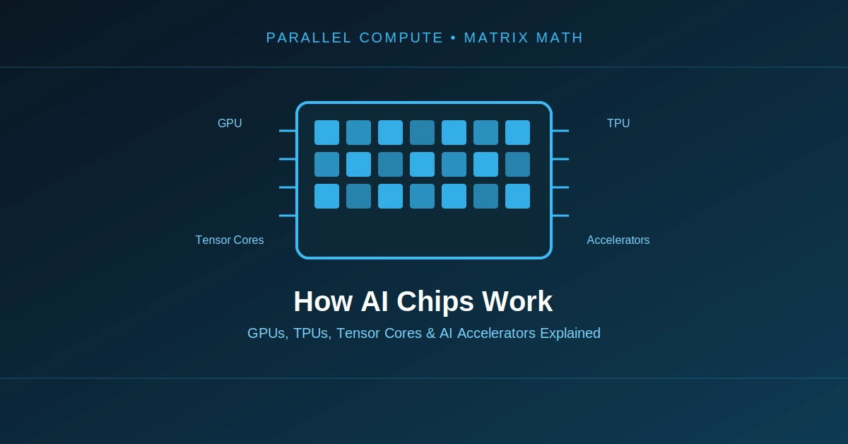
Modern AI hardware includes GPUs with specialized Tensor Cores, dedicated AI accelerators, Google’s TPUs, and neural processing units (NPUs) integrated into consumer devices.
The basic idea is straightforward:
AI model
   ↓
Lots of mathematical operations
   ↓
Matrix / tensor calculations
   ↓
Parallel computation
   ↓
AI accelerator
   ↓
Faster AI workloads
But there is much more happening inside the chip.
What Does an AI Model Actually Calculate?

Before understanding an AI chip, it helps to understand what a neural network is doing mathematically.
A simplified neural-network layer can be represented as:
Output = Input × Weights + Bias
For example:
Input:

[ x1 ]
[ x2 ]
[ x3 ]

        ×

Weights:

[ w11  w12 ]
[ w21  w22 ]
[ w31  w32 ]
The hardware performs many multiplication and addition operations to produce the output.
A neural network contains many such operations.
At large scale, these calculations become matrix multiplications.
Google explains that neural networks perform enormous numbers of multiplications and additions between inputs and model parameters, which can be organized into matrix operations.
This is one of the main reasons AI hardware is built around highly parallel mathematical computation.
Why CPUs Are Not Enough
A CPU is a general-purpose processor.
It is designed to handle a huge variety of workloads:
- operating systems
- web browsers
- databases
- application logic
- file processing
- networking
- games
- scientific calculations
That flexibility is extremely useful.
But neural networks have a different computational pattern.
Imagine a calculation requiring millions of independent multiplication operations.
A CPU might have a relatively small number of powerful general-purpose cores.
An AI accelerator can instead contain a very large number of arithmetic units designed to perform many operations simultaneously.
The difference can be visualized as:
CPU

Core 1  → calculation
Core 2  → calculation
Core 3  → calculation
Core 4  → calculation


AI accelerator

Unit 1   → calculation
Unit 2   → calculation
Unit 3   → calculation
Unit 4   → calculation
Unit 5   → calculation
Unit 6   → calculation
...
Unit N   → calculation
The exact architecture differs between chips, but the important principle is parallelism.
AI workloads often contain huge amounts of parallel mathematical work.
GPUs Became Important for AI
GPUs were originally designed primarily for graphics.
Graphics rendering contains many operations that can be performed simultaneously.
For example, thousands or millions of pixels may need similar calculations.
That made GPUs naturally suitable for parallel workloads.
Researchers eventually discovered that the same parallel computing capabilities could be used for machine learning.
NVIDIA’s CUDA platform helped make general-purpose GPU computing practical for developers, and GPUs became a major platform for deep-learning training and inference.
But modern AI GPUs are no longer simply graphics processors being used for AI.
They contain hardware specifically designed to accelerate AI mathematics.
That is where Tensor Cores come in.
What Are Tensor Cores?
Tensor Cores are specialized processing units inside NVIDIA GPUs designed to accelerate matrix operations used heavily by AI and other high-performance workloads.
NVIDIA describes Tensor Cores as specialized hardware for mixed-precision matrix computation and AI acceleration.
A simplified view looks like:
Modern AI GPU
┌──────────────────────────────┐
│                              │
│  GPU compute units           │
│                              │
│  Tensor Cores                │
│  Tensor Cores                │
│  Tensor Cores                │
│                              │
│  Cache / memory interfaces   │
│                              │
└──────────────────────────────┘
The Tensor Cores are optimized for the kinds of mathematical operations that appear repeatedly in neural networks.
Instead of treating every operation as a completely general-purpose instruction, specialized hardware can execute matrix operations much more efficiently.
What Is a Matrix Multiplication?

Consider two matrices:
A = [ 1  2 ]
    [ 3  4 ]

B = [ 5  6 ]
    [ 7  8 ]
Their multiplication produces:
A × B =
[ 1×5 + 2×7    1×6 + 2×8 ]
[ 3×5 + 4×7    3×6 + 4×8 ]
The result is:
[ 19  22 ]
[ 43  50 ]
Even this tiny example contains several multiplication and addition operations.
Now imagine matrices containing thousands or millions of values.
AI models perform these operations repeatedly.
An AI accelerator is designed to execute large numbers of these calculations efficiently.
Multiply-Accumulate: The Basic AI Operation
A particularly important operation is multiply-accumulate, commonly written as:
a × b + c
For a neural network, the hardware may repeatedly calculate:
a1 × b1
a2 × b2
a3 × b3
...
and accumulate the results:
(a1 × b1) +
(a2 × b2) +
(a3 × b3) +
...
This pattern appears throughout neural-network computation.
Specialized AI hardware can therefore dedicate substantial silicon to performing these operations efficiently.
Why Parallelism Matters
Suppose you have:
1,000,000 independent calculations
You could theoretically process them one after another:
Calculation 1
Calculation 2
Calculation 3
...
Calculation 1,000,000
Or hardware can process many of them simultaneously:
Calculation 1 ──┐
Calculation 2 ──┤
Calculation 3 ──┤
Calculation 4 ──┤
Calculation 5 ──┤──→ Results
Calculation 6 ──┤
Calculation 7 ──┤
Calculation 8 ──┘
This is the fundamental advantage of massively parallel processors for many AI workloads.
But raw arithmetic capacity is only part of the problem.
The chip also needs to feed data to those arithmetic units quickly enough.
Memory Is a Huge Part of AI Computing
An AI accelerator can have thousands of arithmetic units, but those units are useless if they spend most of their time waiting for data.
Consider:
Memory
  ↓
Load data
  ↓
Compute
  ↓
Store result
If memory is too slow, computation units can sit idle.
This creates a major engineering challenge:
How do you move enormous amounts of data to the compute units without wasting too much time or energy?
Modern AI chips therefore use multiple levels of memory and cache.
A simplified hierarchy looks like:
High-capacity system memory
          ↓
High-bandwidth accelerator memory
          ↓
On-chip cache / SRAM
          ↓
Registers / local storage
          ↓
Compute units
The closer memory is to the computation, the faster it can generally be accessed, but on-chip memory is also much more limited in capacity.
High-Bandwidth Memory
Large AI accelerators often use High Bandwidth Memory (HBM).
HBM provides very high memory bandwidth, allowing large amounts of model data and intermediate results to move between memory and compute hardware.
Google’s current TPU documentation, for example, lists HBM capacity and bandwidth as important parts of TPU architecture.
This matters because large AI models contain enormous numbers of parameters.
If the hardware cannot move those parameters and activations efficiently, the arithmetic units cannot remain fully utilized.
The Memory Wall
This problem is often described as the memory wall.
Imagine a chip capable of performing enormous numbers of calculations per second.
But suppose moving the required data from memory takes too long.
Then the theoretical compute performance does not translate directly into real-world performance.
Conceptually:
                    AI workload
                        │
             ┌──────────┴──────────┐
             ↓                     ↓
         Compute                 Memory
             │                     │
      Very high speed       Data movement
             │                     │
             └──────────┬──────────┘
                        ↓
                  Actual performance
This is why AI chip design is not simply about adding more arithmetic units.
Memory bandwidth, cache, interconnects, data reuse and software scheduling are equally important.
What Is a TPU?
A Tensor Processing Unit (TPU) is Google’s custom AI accelerator.
Google describes TPUs as application-specific integrated circuits designed specifically to accelerate machine-learning workloads, particularly the large matrix operations common in neural networks.
A simplified TPU architecture looks like:
                 TPU
                  │
       ┌──────────┼──────────┐
       ↓          ↓          ↓
   Matrix       Vector      Scalar
   units        units       units
       │
       ↓
     HBM
       │
       ↓
   Interconnect
Modern TPU designs contain specialized matrix-multiplication hardware along with vector and scalar processing resources.
For example, Google documents TPU v6e as containing a TensorCore with matrix-multiply units, a vector unit and a scalar unit.
The exact architecture changes between generations, but the basic philosophy remains: build hardware optimized for machine-learning computation.
What Is a Systolic Array?
One of the most interesting ideas in specialized AI hardware is the systolic array.
A systolic array connects many arithmetic units so that data can flow through them in a predictable pattern.
A simplified representation:
Input
  ↓
┌───┐ → ┌───┐ → ┌───┐ → ┌───┐
│MAC│   │MAC│   │MAC│   │MAC│
└───┘   └───┘   └───┘   └───┘
  ↓       ↓       ↓       ↓
┌───┐ → ┌───┐ → ┌───┐ → ┌───┐
│MAC│   │MAC│   │MAC│   │MAC│
└───┘   └───┘   └───┘   └───┘
  ↓       ↓       ↓       ↓
Output
Here, MAC means multiply-accumulate.
Instead of repeatedly fetching and storing intermediate values, the architecture can pass data between neighboring compute units.
Google’s TPU architecture documentation explains that systolic arrays allow matrix calculations to flow through many arithmetic units while reusing data, reducing some of the memory movement associated with conventional architectures.
This is a major idea in specialized AI hardware:
Do more computation while moving less data.
Why Data Reuse Matters
Suppose the same value is needed by many calculations.
A poorly designed system might repeatedly load that value from memory.
A more specialized architecture can keep the value close to the computation and reuse it.
Conceptually:
Traditional approach:

Memory → Compute
Memory → Compute
Memory → Compute
Memory → Compute


Data-reuse approach:

Memory
  ↓
Compute → Compute → Compute → Compute
The second approach can significantly reduce data movement.
And data movement consumes both time and energy.
AI Chips Use Different Numerical Precisions
AI models do not always need every calculation to use the highest numerical precision available.
Traditional scientific computing often uses 32-bit floating-point numbers, commonly called FP32.
AI workloads can frequently use lower-precision formats while maintaining acceptable model accuracy.
Examples include:
FP32
BF16
FP16
FP8
INT8
INT4
The exact formats supported depend on the hardware and workload.
NVIDIA’s Tensor Cores support multiple precision modes, including lower-precision formats designed to increase AI throughput while managing accuracy.
The basic trade-off is:
Higher precision
      ↓
More numerical detail
      ↓
Usually more memory / compute cost


Lower precision
      ↓
Less data per value
      ↓
Potentially higher throughput
      ↓
Lower memory requirements
This is one reason modern AI chips can perform enormous numbers of operations per second.
What Is Quantization?
Quantization takes the precision idea further.
A model’s weights or activations can sometimes be represented using fewer bits.
For example:
FP16 → 16 bits
INT8 → 8 bits
INT4 → 4 bits
Using fewer bits can reduce memory requirements and potentially increase computational efficiency.
However, quantization is not free.
If numerical precision is reduced too aggressively, model quality can degrade.
So engineers need to balance:
Accuracy
   ↕
Performance
   ↕
Memory
   ↕
Power
Google has also described quantization as a technique that can reduce the memory and computational resources required for neural-network inference.
Training vs Inference
AI chips are used for both training and inference, but the workloads are different.
Training
During training, the model learns its parameters.
The process involves:
Input data
    ↓
Forward pass
    ↓
Prediction
    ↓
Loss calculation
    ↓
Backward pass
    ↓
Gradient calculation
    ↓
Weight update
This happens repeatedly over enormous datasets.
Training therefore requires massive amounts of computation and memory bandwidth.
Inference
During inference, the trained model is used to generate an output.
For example:
Prompt
  ↓
Model
  ↓
Prediction
  ↓
Generated response
Inference can have different optimization requirements, particularly around latency, throughput and memory.
The same accelerator may support both workloads, but the best hardware configuration and software strategy can differ.
How an AI Chip Runs an LLM
Consider a simplified language model.
You type:
Explain how semiconductors work.
The system first converts the text into tokens.
The model then processes those tokens through its neural-network layers.
A simplified transformer pipeline is:
Text
 ↓
Tokenization
 ↓
Token IDs
 ↓
Embeddings
 ↓
Transformer layers
 ↓
Matrix operations
 ↓
Attention
 ↓
MLP operations
 ↓
Output probabilities
 ↓
Next token
The AI accelerator is responsible for a huge portion of the numerical work in those layers.
The hardware repeatedly performs operations involving:
- matrix multiplication
- vector operations
- additions
- normalization
- activation functions
- attention calculations
- memory movement
The exact workload varies between models and architectures.
Attention Is Also a Hardware Problem
Transformers rely heavily on attention.
At a simplified level, attention involves calculations using:
Q = Query
K = Key
V = Value
The system calculates relationships between tokens and uses those relationships to determine which information should influence the next computation.
That creates more matrix operations.
So when an AI accelerator is advertised as being good at transformer workloads, it is not simply “running AI.”
It is accelerating the underlying mathematical operations that transformers perform.
AI Chips Need Fast Interconnects
One AI accelerator may not be enough for a large model.
A modern training system can use many accelerators.
For example:
GPU ─── GPU ─── GPU ─── GPU
 │       │       │       │
 ├───────┼───────┼───────┤
 │       │       │       │
GPU ─── GPU ─── GPU ─── GPU
The chips need to communicate with one another.
This creates another bottleneck.
If computation is extremely fast but communication between accelerators is slow, the system can spend significant time waiting for data.
Google’s current TPU systems use specialized high-speed interconnects to connect large numbers of accelerator chips into larger computing systems.
Modern AI infrastructure is therefore a combination of:
Compute
+
Memory
+
Interconnect
+
Software
Not just the chip itself.
Why AI Chips Are Often Called Accelerators
The word accelerator is important.
An accelerator is usually not intended to replace the CPU completely.
Instead, the CPU can manage general application logic while specialized hardware handles computationally intensive workloads.
A simplified system could look like:
              CPU
               │
       ┌───────┴────────┐
       │                │
       ↓                ↓
   Application       AI accelerator
                        │
                        ↓
                 Neural-network
                   computation
The CPU might handle:
- operating-system tasks
- application logic
- data preparation
- scheduling
- control
The accelerator handles the heavy numerical workload.
This division allows each type of hardware to perform the work it is designed for.
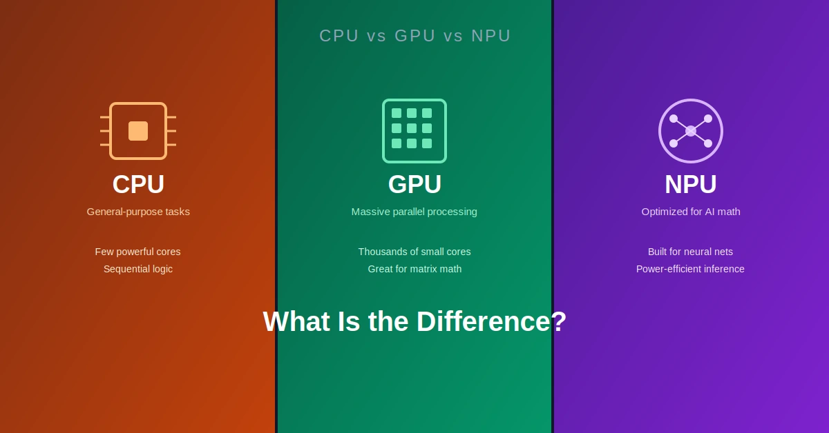
What About NPUs?
You may also encounter another term:
NPU — Neural Processing Unit.
NPUs are specialized processors designed to accelerate AI and machine-learning workloads, particularly on devices such as smartphones and PCs.
The basic idea is similar to other AI accelerators:
CPU → General-purpose work
GPU → Graphics + highly parallel workloads
NPU → AI-specific workloads
The boundaries are not always this simple.
Modern CPUs and GPUs can contain AI-specific instructions or accelerator blocks, while NPUs can support a variety of operations.
The important difference is the design target.
An NPU is generally optimized around efficient execution of neural-network workloads, especially where power efficiency matters.
Why AI Chips Care So Much About Power
AI computation requires enormous amounts of electricity at scale.
A data center running thousands of accelerators cannot treat power consumption as an afterthought.
Every operation requires energy.
But moving data can also consume substantial energy.
This is why AI-chip designers focus heavily on:
- computational efficiency
- memory efficiency
- data reuse
- lower precision
- specialized hardware
- cooling
- interconnect efficiency
The objective is not simply:
Maximum calculations
It is often closer to:
Maximum useful AI work
per watt
This is why performance-per-watt is an important metric when evaluating AI accelerators.
AI Chip Performance Is More Than TOPS or FLOPS
AI chips are often advertised using numbers such as:
TFLOPS
PFLOPS
TOPS
These represent theoretical computational throughput under particular numerical formats and conditions.
But a higher theoretical number does not automatically mean a model will run proportionally faster.
Real performance also depends on:
- model architecture
- numerical precision
- memory bandwidth
- memory capacity
- batch size
- software libraries
- compiler optimization
- interconnect
- workload characteristics
- utilization
For example:
Chip A
1000 units of theoretical compute

Chip B
800 units of theoretical compute
Chip A is not automatically faster for every AI workload.
If Chip B has better memory behavior or software optimization for the particular model, its real-world performance can be different.
The Software Behind the AI Chip
Hardware alone does not make an AI accelerator useful.
The software stack needs to translate high-level AI operations into efficient hardware execution.
A simplified stack looks like:
AI application
      ↓
PyTorch / JAX / other framework
      ↓
Compiler
      ↓
Kernel libraries
      ↓
Hardware instructions
      ↓
AI accelerator
Google’s TPU stack, for example, uses the XLA compiler to transform operations from supported machine-learning frameworks into code suitable for TPU execution.
NVIDIA’s ecosystem similarly provides CUDA and optimized libraries that allow AI frameworks to use GPU acceleration.
This hardware-software relationship is extremely important.
A theoretically powerful chip can be difficult to use efficiently if the software ecosystem does not support the workloads developers care about.
Why AI Chips Are Becoming More Specialized
AI models are changing.
Early neural-network workloads were dominated by relatively straightforward dense matrix operations.
Modern models can involve:
- transformers
- mixture-of-experts architectures
- long-context processing
- sparse operations
- recommendation models
- multimodal models
- generative image models
- reasoning workloads
Hardware therefore increasingly contains specialized units for different types of operations.
Google’s recent TPU architectures, for example, combine matrix-multiplication hardware with vector, scalar and specialized components for workloads such as embeddings.
The trend is toward heterogeneous computing.
Instead of one type of processing unit doing everything, different units handle different workloads.
A Simplified Modern AI Chip
Putting everything together:
                 AI Accelerator
┌────────────────────────────────────────┐
│                                        │
│  Matrix / Tensor Compute               │
│  ┌────┐ ┌────┐ ┌────┐ ┌────┐          │
│  │MAC │ │MAC │ │MAC │ │MAC │   ...    │
│  └────┘ └────┘ └────┘ └────┘          │
│                                        │
│  Vector / Scalar Processing            │
│                                        │
│  Cache / SRAM                           │
│                                        │
│  Memory Controllers                     │
│                                        │
└───────────────┬────────────────────────┘
                │
                ↓
              HBM
                │
                ↓
        High-speed interconnect
The exact design varies dramatically between NVIDIA GPUs, Google TPUs, smartphone NPUs and other accelerators.
But the basic objective remains the same:
Keep large amounts of computation running efficiently while moving data through the system as efficiently as possible.
How an AI Chip Generates an AI Response
We can now simplify the entire process.
Suppose you ask an AI model:
What is a semiconductor?
The system might perform something conceptually like:
User prompt
    ↓
Tokenization
    ↓
Input tokens
    ↓
Move data to accelerator
    ↓
Neural-network computation
    ↓
Matrix multiplication
    ↓
Attention
    ↓
More matrix operations
    ↓
Output probabilities
    ↓
Select next token
    ↓
Repeat
    ↓
Generated response
Behind that simple chat interface, the accelerator may execute an enormous number of mathematical operations.
The AI chip does not “understand” the question in the human sense.
It performs the numerical computations required by the trained model.
Final Takeaway
AI chips work by exploiting the mathematical structure of neural networks.
Instead of treating AI computation like ordinary software execution, specialized hardware dedicates enormous amounts of silicon to parallel numerical operations such as matrix multiplication and multiply-accumulate calculations.
The basic chain is:
AI model
   ↓
Matrix / tensor operations
   ↓
Parallel computation
   ↓
Tensor cores / matrix units
   ↓
Fast memory
   ↓
High-speed interconnect
   ↓
AI result
GPUs, TPUs and NPUs approach this problem differently, but they share the same fundamental goal: perform the calculations required by AI models faster and more efficiently than a general-purpose processor could do alone.
The most important part is not simply having more arithmetic units.
A successful AI accelerator has to balance:
- compute
- memory bandwidth
- memory capacity
- data reuse
- numerical precision
- power consumption
- interconnect
- compiler and software support
That is why an AI chip is much more than a collection of fast processors.
It is a complete computing architecture designed around one of the central problems of modern AI: how to perform enormous amounts of mathematical computation while moving as little unnecessary data as possible.
And as AI models continue to grow, the competition is increasingly not just about who can build the fastest processor, but who can build the most efficient combination of compute, memory, networking and software.
SiliconeUpdate.com is a technology news platform that publishes updates and informational content related to silicon technology, software, artificial intelligence, and emerging technologies.
All articles published on this platform are attributed to SiliconeUpdate.com instead of individual authors. Content is presented in a neutral, informational format without personal opinions.
—
Content Publishing
SiliconeUpdate.com publishes news and updates based on publicly available information, official announcements, and industry developments. The focus is on clarity, relevance, and timely reporting.
—
Editorial Control
All editorial decisions, updates, and content management are handled at the platform level. No individual human or AI identity is presented as the author of articles.
—
Contact
For editorial communication or general queries, contact:
Email: neemasharma@gmail.com