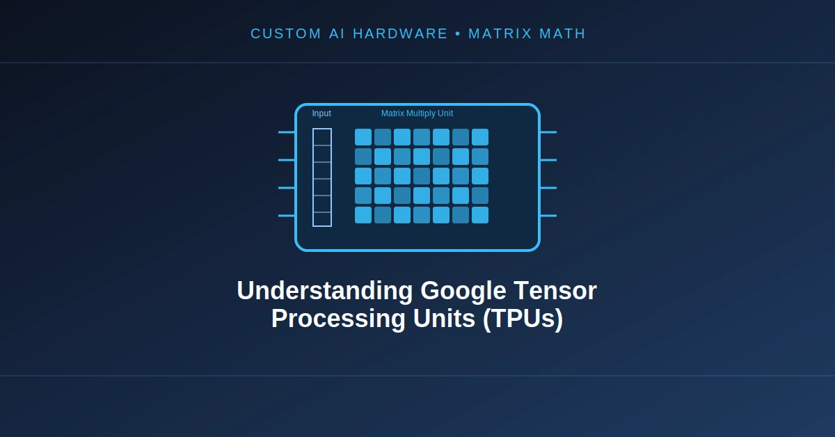
Google’s Tensor Processing Units (TPUs) represent a specialized class of hardware accelerators designed specifically for artificial intelligence (AI) workloads. Unlike general-purpose central processing units (CPUs) or graphics processing units (GPUs), TPUs are engineered from the ground up to optimize the mathematical operations fundamental to machine learning, particularly deep learning. This focus allows them to achieve superior performance and energy efficiency for AI model training and inference.
Purpose-Built for AI
TPUs are custom chips developed by Google. Their design targets the specific mathematical computations prevalent in AI models, primarily large-scale matrix multiplications. This specialization enables them to execute these operations faster and with greater energy efficiency compared to more versatile processors. The architecture prioritizes throughput for tensor operations, which are multi-dimensional data arrays central to neural networks.
Architectural Philosophy
The core philosophy behind TPUs is to accelerate tensor operations by integrating a large number of arithmetic units directly onto the chip. This contrasts with traditional CPU designs that prioritize flexibility across diverse workloads or GPU designs that offer parallel processing for graphics and general-purpose computing. TPUs achieve their efficiency through a streamlined instruction set and a direct pipeline for tensor computations, minimizing overhead.
How TPUs Process AI Workloads
TPUs leverage a unique architecture to accelerate AI computations. Their design is optimized for the repetitive, high-volume matrix operations that characterize neural network training and inference. This specialized approach allows for significant performance gains over general-purpose hardware.
Matrix Multiplication Focus
At the heart of AI models, especially deep neural networks, are extensive matrix multiplications. TPUs are engineered to perform these operations with extreme efficiency. They integrate dedicated hardware units that can execute multiple multiplications and additions concurrently, a process often referred to as a multiply-accumulate (MAC) operation. This direct hardware support bypasses the need for complex instruction decoding and scheduling found in general-purpose processors.
Systolic Array Design
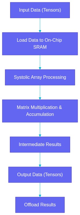
A key architectural feature of TPUs is the systolic array. This is a network of interconnected processing units that can perform parallel computations on data flowing through them. Data streams through the array, and each processing unit performs a calculation before passing the result to the next unit. This design minimizes data movement, which is a significant bottleneck in traditional architectures, and maximizes the utilization of the arithmetic units. The systolic array allows for continuous data processing, leading to high throughput for tensor operations.
On-Chip Memory and Interconnect
TPUs incorporate substantial amounts of on-chip memory, specifically SRAM (Static Random-Access Memory), to reduce latency. By keeping frequently accessed data close to the processing units, the need to fetch data from slower off-chip memory is minimized. For instance, the TPU 8i triples on-chip SRAM to further reduce latency for AI tasks. Additionally, advanced interconnects, such as the Virgo Network topology in the TPU 8t, enable massive scaling, allowing up to 1 million chips to operate cohesively. This network facilitates high-bandwidth communication between individual TPU chips, forming powerful supercomputers for large-scale AI model training.

Photo by Google DeepMind on Pexels
Evolution and Generations of TPUs
Google has continuously evolved its TPU architecture, releasing multiple generations since their initial introduction. Each iteration brings improvements in performance, efficiency, and scalability, solidifying Google’s position in AI hardware.
Early Generations and Cloud Integration
Google initially deployed TPUs internally for its own AI services, such as Google Search and Google Photos. The first generation TPUs were primarily inference accelerators. Subsequent generations, like TPU v2 and v3, were made available through Google Cloud Platform, enabling external developers and researchers to leverage their power for both training and inference. This cloud-first strategy democratized access to specialized AI hardware.
Recent TPU Advancements
The development of TPUs has progressed rapidly, with Google consistently pushing the boundaries of AI chip design. These advancements aim to address the increasing computational demands of larger and more complex AI models. Each new generation typically offers higher computational throughput, improved energy efficiency, and enhanced memory capabilities.
TPU Series 8: Virgo and SRAM Enhancements
Google’s latest offerings include the TPU 8t and TPU 8i AI chips. The TPU 8t features the advanced Virgo Network topology, which is critical for scaling AI infrastructure. This topology allows for the interconnection of up to 1 million chips, creating immense computational clusters for training extremely large models. The TPU 8i focuses on reducing latency for AI inference and smaller training tasks by tripling its on-chip SRAM. This increased local memory minimizes data transfer bottlenecks, leading to faster response times.
TPU Ecosystem and Strategic Collaborations
The impact of Google’s TPUs extends beyond their technical specifications, influencing the broader AI hardware landscape and fostering strategic industry partnerships. Their development represents a significant move to gain an edge in AI computing.
Scalability with Virgo Network Topology
The Virgo Network topology, introduced with the TPU 8t, is a foundational element for building hyperscale AI infrastructure. This network design facilitates seamless communication and data sharing across a vast number of TPU chips. The ability to scale up to 1 million interconnected chips provides an unparalleled platform for developing and deploying the next generation of AI models, offering Google a distinct advantage in AI development.
Industry Impact and Partnerships
TPUs pose a significant challenge to established players in the AI chip market, such as Nvidia. Their specialized design and Google’s strategic deployment give Google an edge in AI. Google’s reported work with AMD on a 10th-generation TPU signifies a potential collaboration that could reshape AI chip design and reduce the industry’s dependence on GPUs for AI workloads. This partnership highlights the ongoing evolution and competitive nature of the AI hardware sector.
| Feature | TPU 8t | TPU 8i |
|---|---|---|
| Primary Focus | Large-scale Training | Inference & Latency Reduction |
| Network Topology | Virgo Network | Standard Interconnect |
| Scaling Capability | Up to 1 million chips | Optimized for individual/smaller clusters |
| On-Chip SRAM | Standard (relative to 8t’s scale) | Tripled for reduced latency |
| Key Benefit | Massive model training | Faster inference, lower latency |

Photo by Google DeepMind on Pexels
Key Takeaways
- Google TPUs are custom-designed AI accelerators optimized for the matrix multiplication operations central to machine learning.
- Their architecture features systolic arrays, which efficiently process data streams and minimize data movement for high throughput.
- TPUs integrate substantial on-chip SRAM and advanced interconnects like the Virgo Network to reduce latency and enable massive scalability.
- The TPU 8t utilizes the Virgo Network to scale up to 1 million chips for large-scale training, while the TPU 8i triples SRAM for reduced inference latency.
- Google’s continuous TPU development and strategic collaborations, such as with AMD for a 10th-generation chip, position them as a significant force in the AI hardware market.
The specialized systolic array architecture of TPUs allows them to achieve high computational density and energy efficiency by keeping data movement to a minimum, a critical factor for AI workloads.
Real World Example
Consider a large language model (LLM) undergoing training with billions of parameters. This process involves an immense number of matrix multiplications and requires vast computational resources. A single Google TPU 8t pod, leveraging the Virgo Network topology, can interconnect numerous individual TPU 8t chips. This creates a unified, high-bandwidth computing environment capable of distributing the model’s parameters and training data across the entire cluster. The systolic arrays within each chip efficiently process the tensor operations, while the tripled on-chip SRAM in companion TPU 8i units might handle specific, latency-sensitive inference tasks once the model is trained. This integrated approach allows Google to train and deploy state-of-the-art AI models with unprecedented speed and scale.
Frequently Asked Questions
What is the primary advantage of a Google TPU over a GPU for AI?
TPUs are custom-designed for the specific math operations of AI, particularly matrix multiplication, making them faster and more energy-efficient for these tasks. GPUs are more general-purpose parallel processors, originally designed for graphics rendering.
How does a systolic array contribute to TPU performance?
A systolic array is a grid of processing units that allows data to flow continuously through the chip, performing calculations at each step. This design minimizes data movement, reducing bottlenecks and maximizing the utilization of arithmetic units for high throughput.
What is the significance of the Virgo Network topology in TPU 8t?
The Virgo Network topology enables the TPU 8t to scale up to 1 million interconnected chips. This massive scalability is crucial for training extremely large and complex AI models, providing a unified computational platform.
Are Google TPUs available for external use?
Yes, Google makes its TPUs available through the Google Cloud Platform. This allows researchers and developers to access and utilize TPU resources for their AI model training and inference workloads without needing to acquire physical hardware.
SiliconeUpdate.com is a technology news platform that publishes updates and informational content related to silicon technology, software, artificial intelligence, and emerging technologies.
All articles published on this platform are attributed to SiliconeUpdate.com instead of individual authors. Content is presented in a neutral, informational format without personal opinions.
—
Content Publishing
SiliconeUpdate.com publishes news and updates based on publicly available information, official announcements, and industry developments. The focus is on clarity, relevance, and timely reporting.
—
Editorial Control
All editorial decisions, updates, and content management are handled at the platform level. No individual human or AI identity is presented as the author of articles.
—
Contact
For editorial communication or general queries, contact:
Email: neemasharma@gmail.com